Solid-state image sensor and method for fabricating the same

a solid-state image sensor and image sensor technology, applied in separation processes, television systems, radio frequency controlled devices, etc., can solve the problems of large impurity region in the depth length of the silicon substrate b>50/b>, implantation defects may be generated, and the implantation defect generation range is reduced, surface leak current reduction, and the effect of improving the sensitivity to blue light having a short wavelength

Inactive Publication Date: 2006-04-27
SHARP KK
View PDF7 Cites 32 Cited by
  • Summary
  • Abstract
  • Description
  • Claims
  • Application Information

AI Technical Summary

Benefits of technology

[0030] According to the present invention, a solid-state image sensor such as a MOS image sensor includes a plurality of unit pixel portions provided in a two-dimensional array. Each of the unit pixel portions includes a light receiving area, an electric storage area and a transistor. In such a solid-state image sensor, the maximum impurity concentration portion of a second conductive type semiconductor layer region of a surface of the light receiving area is at a surface of a first conductive type substrate. Thus, generation of implantation defects in the light receiving area is reduced and a surface leak current can be reduced. Further, since the surface-generated leak current due to the second conductive type semiconductor layer region is reduced in the surface of the first conductive type substrate of the light receiving area, the sensitivity to blue light having a short wavelength can be improved in the second conductive type semiconductor layer below the surface of the first conductive type substrate.
[0031] In the fabrication method for the solid-state image sensor according to the present invention, ion implantation is performed with having an insulation film such as thermal oxidation film as an implantation protection film so as to cover the substrate surface, and the second conductive type semiconductor layer region of the surface of the light receiving area is formed. Thus, a surface leak current due to surface defects on the surface of the light receiving area can be reduced, and the properties in the light receiving area can be improved. As a result, the sensitivity to blue light having a short wavelength can be improved.
[0032] Thus, the invention described herein makes possible the advantages of providing: a solid-state image sensor which can reduce defects generated by ion implantation in a light receiving area and can reduce a surface leak current due to photo-generated electric charges at a surface of the light receiving area; and a fabrication method thereof.

Problems solved by technology

This cause problems that a variance in an ion implantation range when ions are implanted (ARp) becomes large and an extent of the impurity region in the depth length of the silicon substrate 50 becomes large.
Further, if an average range when ion implantation impurities are implanted is set to a position deep inside from the surface of the silicon substrate 50, implantation defects may be generated in the light receiving diode 60 and a surface leak current may be undesirably generated.
Moreover, when the gate electrode 52 is formed by using a plasma process, if plasma gives damage on an upper-most surface of the light receiving diode 60, a surface leak current due to surface defects may be undesirably generated.

Method used


Image

  • Solid-state image sensor and method for fabricating the same
  • Solid-state image sensor and method for fabricating the same
  • Solid-state image sensor and method for fabricating the same

Examples


Embodiment Construction

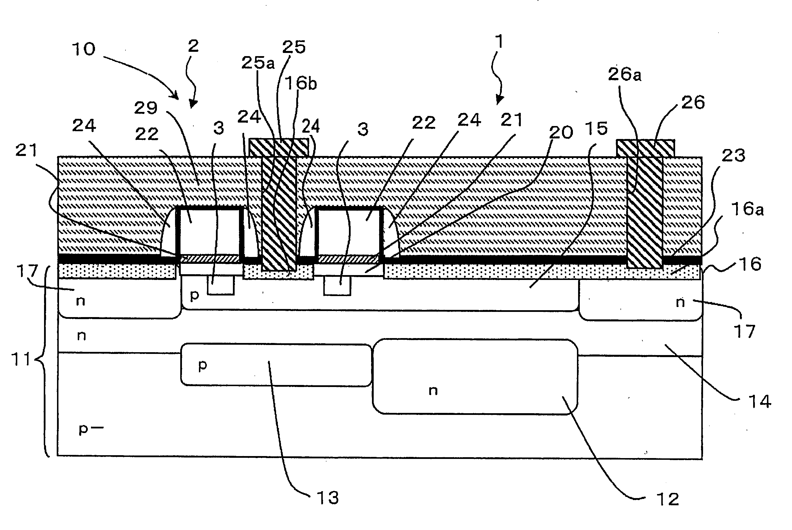
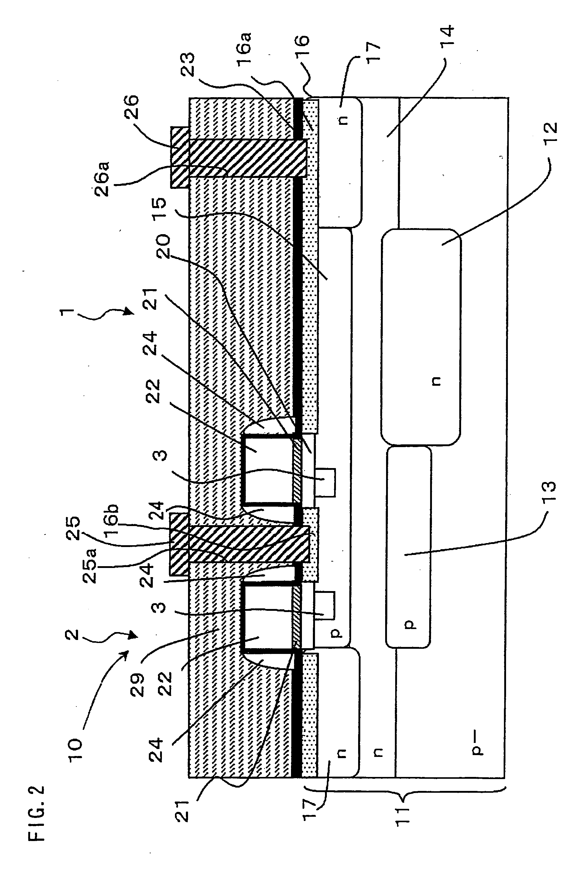
[0041] Hereinafter, embodiments of a solid-state image sensor and a fabrication method thereof according to the present invention when applied to a MOS-type image sensor of a threshold voltage modulation type will be described with reference to the drawings. The solid-state image sensor of the present invention is not limited to a MOS-type image sensor.

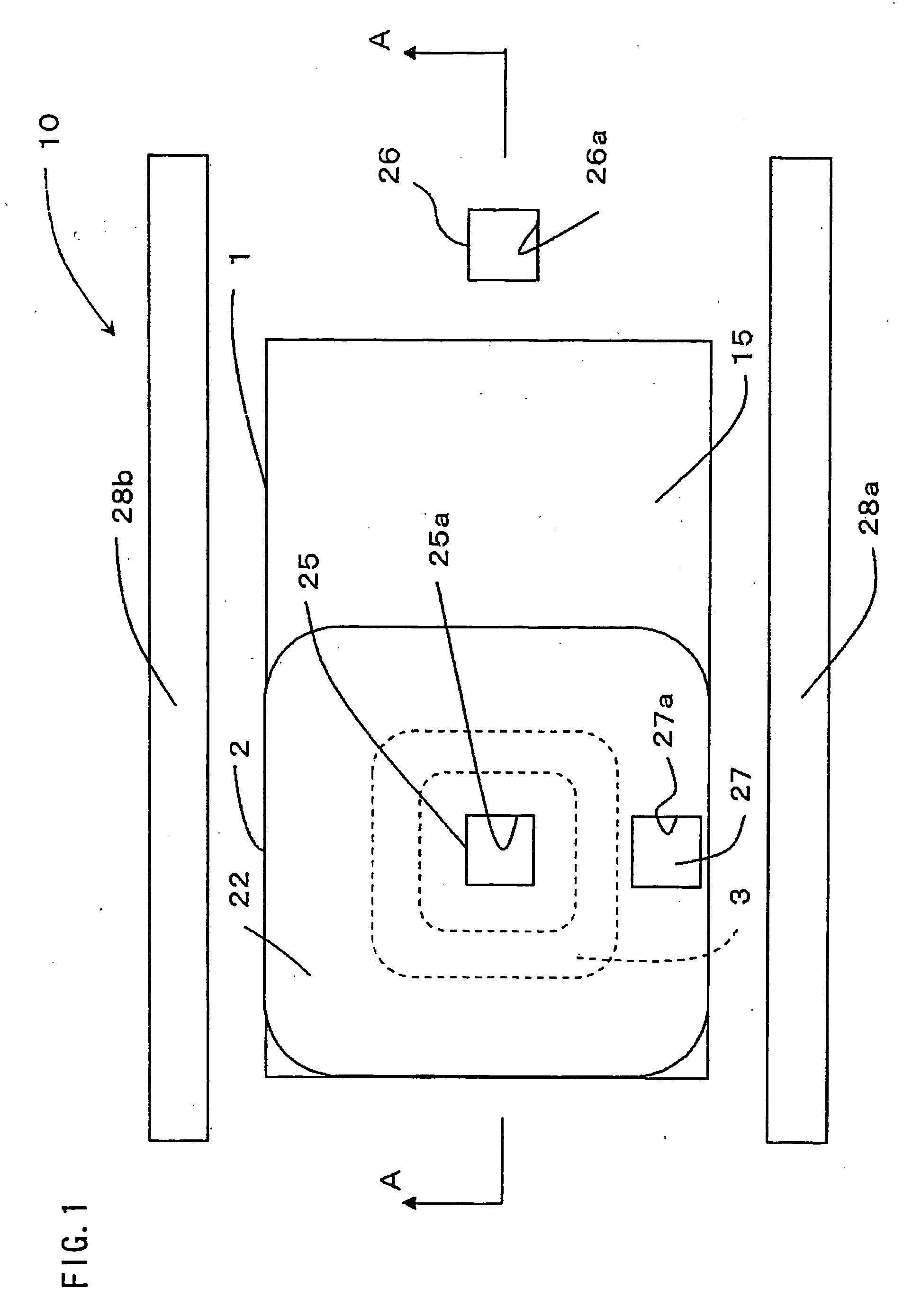
[0042]FIG. 1 is a plan view showing an exemplary layout of a unit pixel portion 10 in a MOS-type image sensor which is one embodiment of the solid-state image sensor according to the present invention. FIG. 2 is a cross-sectional view along A-A line in FIG. 1. Although not shown in FIGS. 1 and 2, in the MOS-type image sensor (solid-state image sensor), a plurality of unit pixel portions are arranged in a matrix (two-dimensional array) in a row direction and a column direction.

[0043] The unit pixel portion 10 of the MOS-type image sensor shown in FIGS. 1 and 2 includes: a light receiving diode (photodiode) 1 which is a light receivin...


PUM

PropertyMeasurementUnit
thicknessaaaaaaaaaa
depthaaaaaaaaaa
thicknessaaaaaaaaaa

Abstract

A solid-state image sensor in which a plurality of unit pixel portions, each including a light receiving area which generates electric charges by light irradiation and a transistor which outputs an electric signal in accordance with the light receiving area, are arranged in a two-dimensional array, in which: each of the unit pixel portions includes a first conductive type well region provided on a second conductive type semiconductor layer in a first conductive type substrate, a part of the first conductive type well region and a second conductive type semiconductor layer region laminated on a part of the first conductive type well region form the light receiving area; electric charge storage area for storing electric charges generated in the light receiving area is provided in the first conductive type well region to read out an electric signal in accordance with an amount of electric charges stored in the electric charge storage area from the transistor; and the second conductive type semiconductor layer region has a maximum impurity concentration portion in the depth direction of the first conductive type substrate is at a surface of the first conductive type substrate.

Description

[0001] This Nonprovisional application claims priority under 35 U.S.C. §119(a) on Patent Application No. 2004-107904 filed in Japan on Mar. 31, 2004, the entire contents of which are hereby incorporated by reference. BACKGROUND OF THE INVENTION [0002] 1. Field of the Invention [0003] The present invention relates to a solid-state image sensor used for video cameras, digital cameras, cell phones with built-in cameras, and the like, and a fabrication method thereof. More specifically, the present invention relates to a solid-state image sensor such as a MOS-type image sensor of a threshold voltage modulation type and a fabrication method thereof. [0004] 2. Description of the Related Art [0005] Conventionally, CCD type image sensors, MOS type image sensors, and the like are known as solid-state image sensors for converting image light as an image signal into an electric signal. For example, MOS-type image sensors include light-receiving areas for generating electric charges by light ir...

Claims


Application Information

Patent Timeline
Patent Type & Authority Applications(United States)
IPC IPC(8): H01L29/768H01L27/146H01L31/10H04N5/335H04N5/357H04N5/369H04N5/374
CPCH01L27/14689H01L27/14609B01D35/306B01D35/147B01D2201/29B01D2201/16B01D2201/347
Inventor IWATA, HIROSHI
Owner SHARP KK
Why Eureka
Try Eureka