Cold cathode electric field electron emission display device

a display device and electric field technology, applied in the field of cold cathode field emission display, can solve the problems of affecting the display quality, affecting the brightness and size of the display device, and affecting the operation of the field emission device or the anode electrode b>220/b>, so as to achieve the effect of reducing the scale of damage caused on the anode electrode unit by a discharge, reducing the energy to be generated, and fully reducing the cold ca

Inactive Publication Date: 2006-04-27
SONY CORP
View PDF4 Cites 14 Cited by
  • Summary
  • Abstract
  • Description
  • Claims
  • Application Information

AI Technical Summary

Benefits of technology

[0086] In the cold cathode field emission display of the present invention, the basic concept is not that the trigger for a discharge is suppressed but that energy generated between the anode electrode and the cold cathode field emission device is suppressed so that a small-scale discharge, even if it should take place, does not grow to a large-scale discharge. The anode electrode is not formed on the entire surface of the effective field, but is formed in the form of split anode electrode units having smaller areas, so that the electrostatic capacity between the anode electrode unit and the cold cathode field emission device can be decreased and that energy to be generated can be reduced. As a result, the damage caused on the anode electrode unit by a discharge can be effectively decreased in scale.
[0087] Moreover, in the cold cathode field emission display according to the first or third aspect of the present invention, VA / Lg<1 (kV / μm) is satisfied, so that the occurrence of a discharge between the anode electrode units can be reliably decreased. As a result, permanent damages of the anode electrode unit such as vaporization caused on the anode electrode unit due to the above discharge can be fully decreased. Further, in the cold cathode field emission display according to the second or fourth aspect of the present invention, (VA / 7)2×(S / d)≦2250 is satisfied, and in the cold cathode field emission display according to the fifth aspect of the present invention, the size of the anode electrode units is defined, so that permanent damages of the anode electrode unit such as vaporization caused on the anode electrode unit due to a discharge between the anode electrode unit and the cold cathode field emission device can be fully decreased.

Problems solved by technology

For applying the liquid crystal display to a floor-type television receiver, however, it still has problems to be solved concerning a higher brightness and an increase in size.
When the abnormal discharge takes place, not only the display quality is impaired, but also the field emission device or the anode electrode 220 is damaged.
In a general production process of the anode panels AP or the display panels using the anode panels AP, practicing the above control involves great technical difficulties.

Method used


Image

  • Cold cathode electric field electron emission display device
  • Cold cathode electric field electron emission display device
  • Cold cathode electric field electron emission display device

Examples


example 1

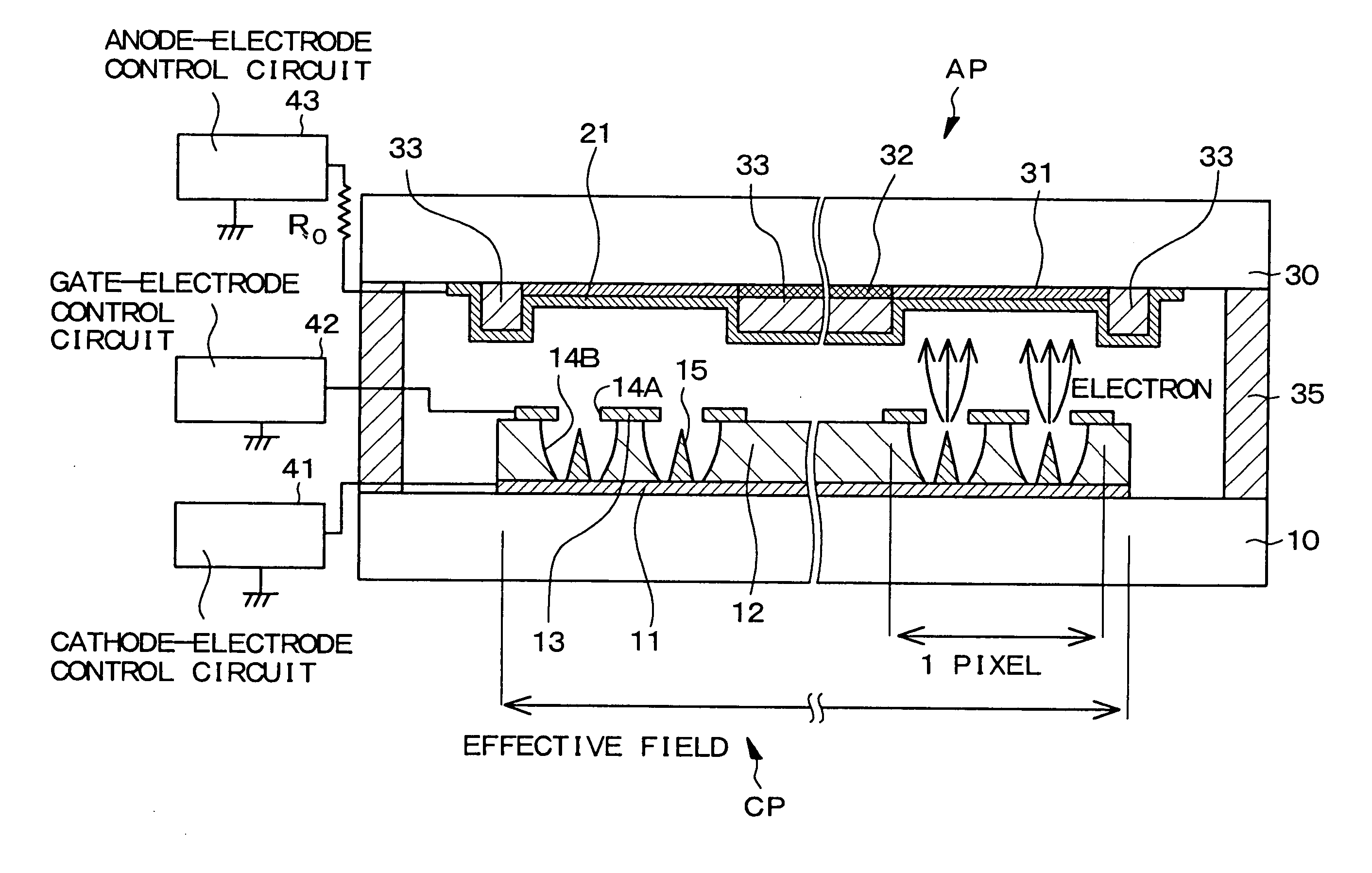
[0118] Example 1 is concerned with the cold cathode field emission display (to be simply abbreviated as “display” hereinafter) according to each of the first, second and fifth aspects of the present invention.

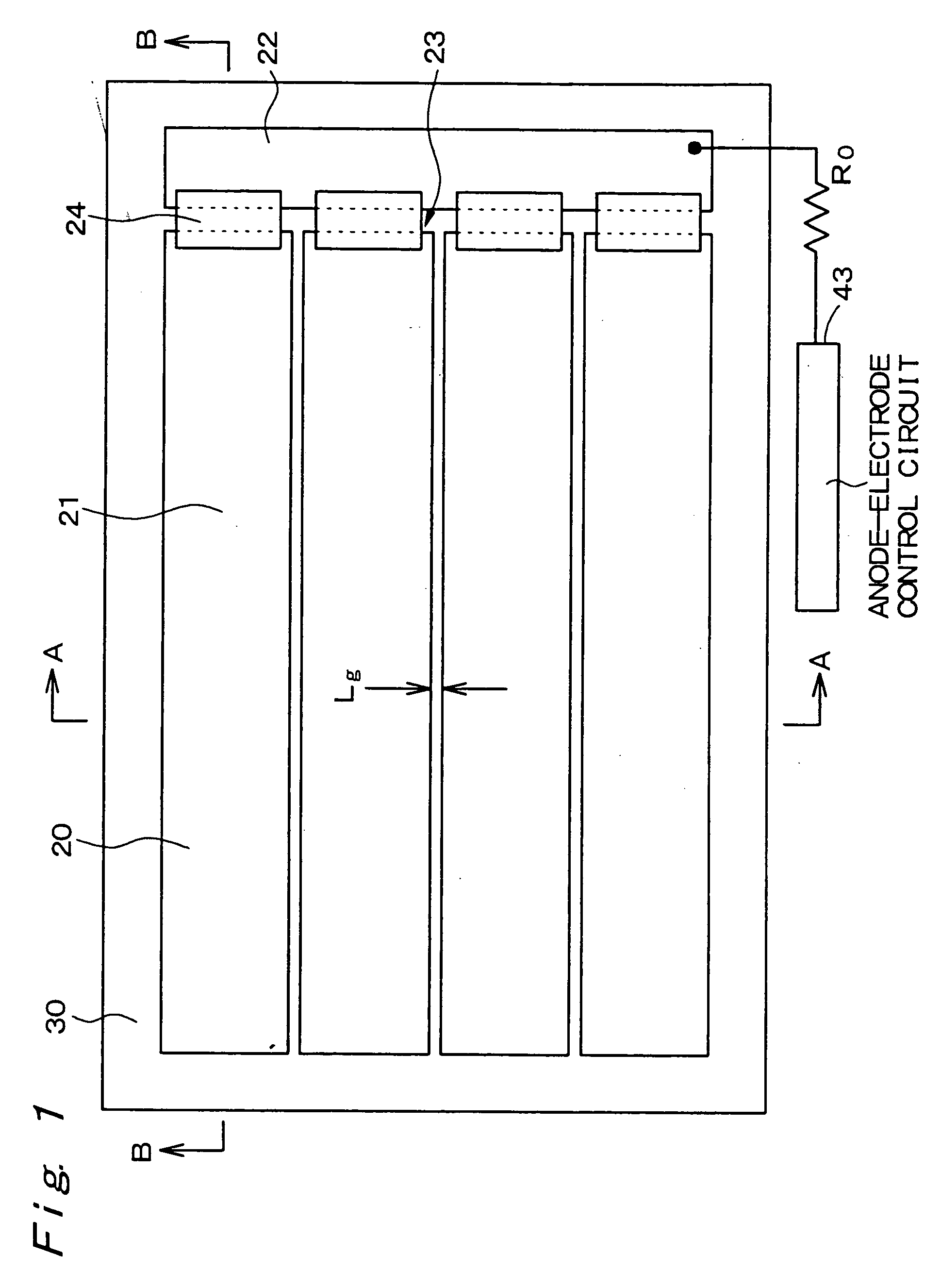
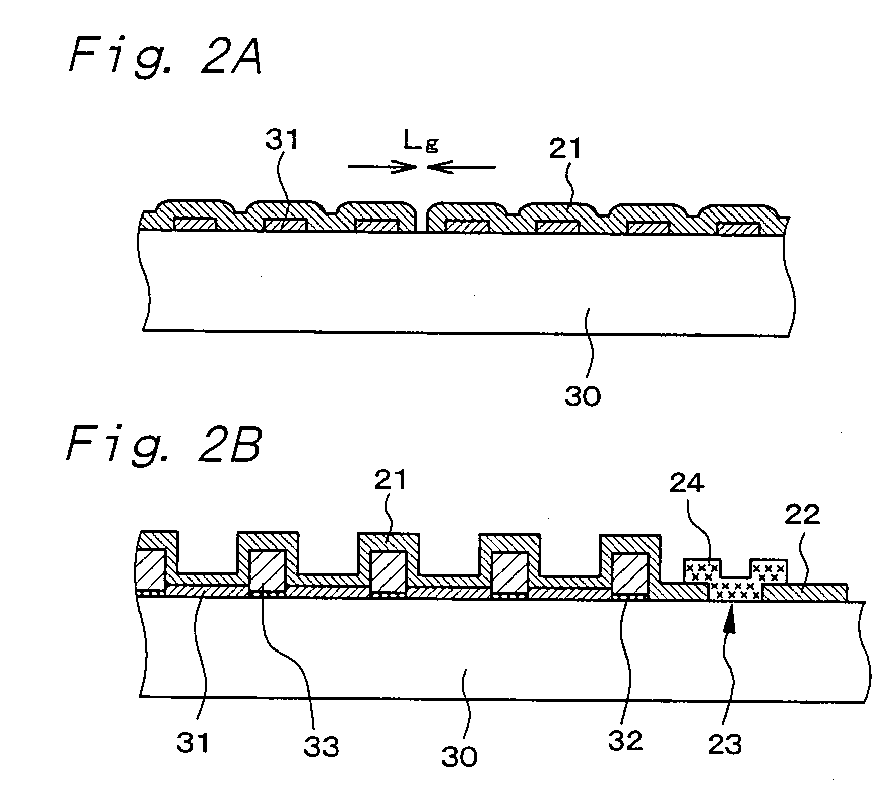
[0119]FIG. 1 shows a schematic plan view of an anode electrode, FIG. 2A shows a schematic partial end view of an anode panel AP taken along line A-A in FIG. 1, and FIG. 2B shows a schematic partial end view of the anode panel AP taken along line B-B in FIG. 1. Further, FIG. 3 shows a schematic partial end view of the display in Example 1, and FIG. 4 shows a partial perspective view of a cathode panel CP. Further, FIGS. 5 to 8 illustrate schematic partial plan views of layouts of phosphor layers and the like. The layout of the phosphor layers, etc., in the schematic partial end view of the anode panel AP has a constitution shown in FIG. 7 or 8.

[0120] The display comprises the cathode panel CP having a plurality of cold cathode field emission devices (to be simply abbreviated a...

example 2

[0141] Example 2 is a variant of Example 1. FIG. 12 shows a schematic partial plan view of an anode panel AP in Example 2, and FIG. 13 shows a schematic partial end view taken along line A-A in FIG. 12. In the anode panel AP in Example 2, an electric supply line 22 is constituted of electric supply line units 22A in the number of M (2≦M≦N, 10M=N in Example 2) connected in series through second resistance elements 26 made of SiC or chromium oxide by a sputtering method. One electric supply line unit 22A is connected to one anode electrode unit 21. The electric supply line unit 22A had a size (area S′) of 1 mm×150 mm. A space 25 is provided between one electric supply line unit 22A and another electric supply line unit 22A, and the second resistance element 26 is formed on the space 25 so as to bridge one electric supply line unit 22A and another electric supply line unit 22A. The second resistance element 26 has a resistance value (r2) of about 5 kilo Ω. The anode panel AP in Example...

example 3

[0144] Example 3 is also a variant of Example 1. FIG. 14A shows a schematic partial end view of an anode panel in Example 3, taken along a line similar to the line A-A in FIG. 1, and FIG. 14B shows a schematic partial end view taken along a line similar to the line B-B in FIG. 1. In Example 3, a stripe-shaped transparent electrode 27 made of ITO and connected to the anode-electrode control circuit 43 is formed between the phosphor layer 31 and the substrate 30. More specifically, a plurality of unit phosphor layers 31 constituting the pixels are arranged in the form of a straight line as shown in FIGS. 5 to 8, and one stripe-shaped transparent electrode 27 connected to the anode-electrode control circuit 43 is formed between one column of a plurality of the unit phosphor layers 31 and the substrate 30. The anode panel AP in Example 3 is structurally the same as the anode panel AP in Example 1 except for the above point, so that a detailed explanation of the anode panel AP, a cathode...


PUM


Abstract

An anode electrode 20 in an anode panel constituting a cold cathode field emission display is constituted of anode electrode units 21 in the number of N (N≧2), each anode electrode unit is connected to an anode-electrode control circuit 43 through one electric supply line 22, and VA/Lg<1 (kV/μm) is satisfied in which VA (unit:kilovolt) is a voltage difference between an output voltage of the anode-electrode control circuit and a voltage applied to a cold cathode field emission device, and Lg (unit:μm) is a gap length between the anode electrode units.

Description

TECHNICAL FIELD [0001] The present invention relates to a cold cathode field emission display having a characteristic feature in an anode electrode provided in an anode panel. BACKGROUND ART [0002] In the fields of displays for use in television receivers and information terminals, studies have been made for replacing conventionally mainstream cathode ray tubes (CRT) with flat-panel displays which are to comply with demands for a decrease in thickness, a decrease in weight, a larger screen and a high fineness. Such flat panel displays include a liquid crystal display (LCD), an electroluminescence display (ELD), a plasma display panel (PDP) and a cold cathode field emission display (FED). Of these, a liquid crystal display is widely used as a display for an information terminal. For applying the liquid crystal display to a floor-type television receiver, however, it still has problems to be solved concerning a higher brightness and an increase in size. In contrast, a cold cathode fie...

Claims


Application Information

Patent Timeline
Patent Type & Authority Applications(United States)
IPC IPC(8): G09G3/10H01J1/304H01J29/28H01J29/92H01J31/12
CPCH01J1/304H01J31/127
Inventor KONISHI, MORIKAZUIIDA, KOICHI
Owner SONY CORP
Why Eureka
Try Eureka