[0015] Certain embodiments of the invention have other advantages in addition to or in place of those mentioned above. The advantages will become apparent to those skilled in the art from a reading of the following detailed description when taken with reference to the accompanying drawings.
[0017]FIG. 2 shows the structure of FIG. 1 with a gate formed thereon;
[0018]FIG. 3 shows the structure of FIG. 2 with a liner and spacer deposited thereon;
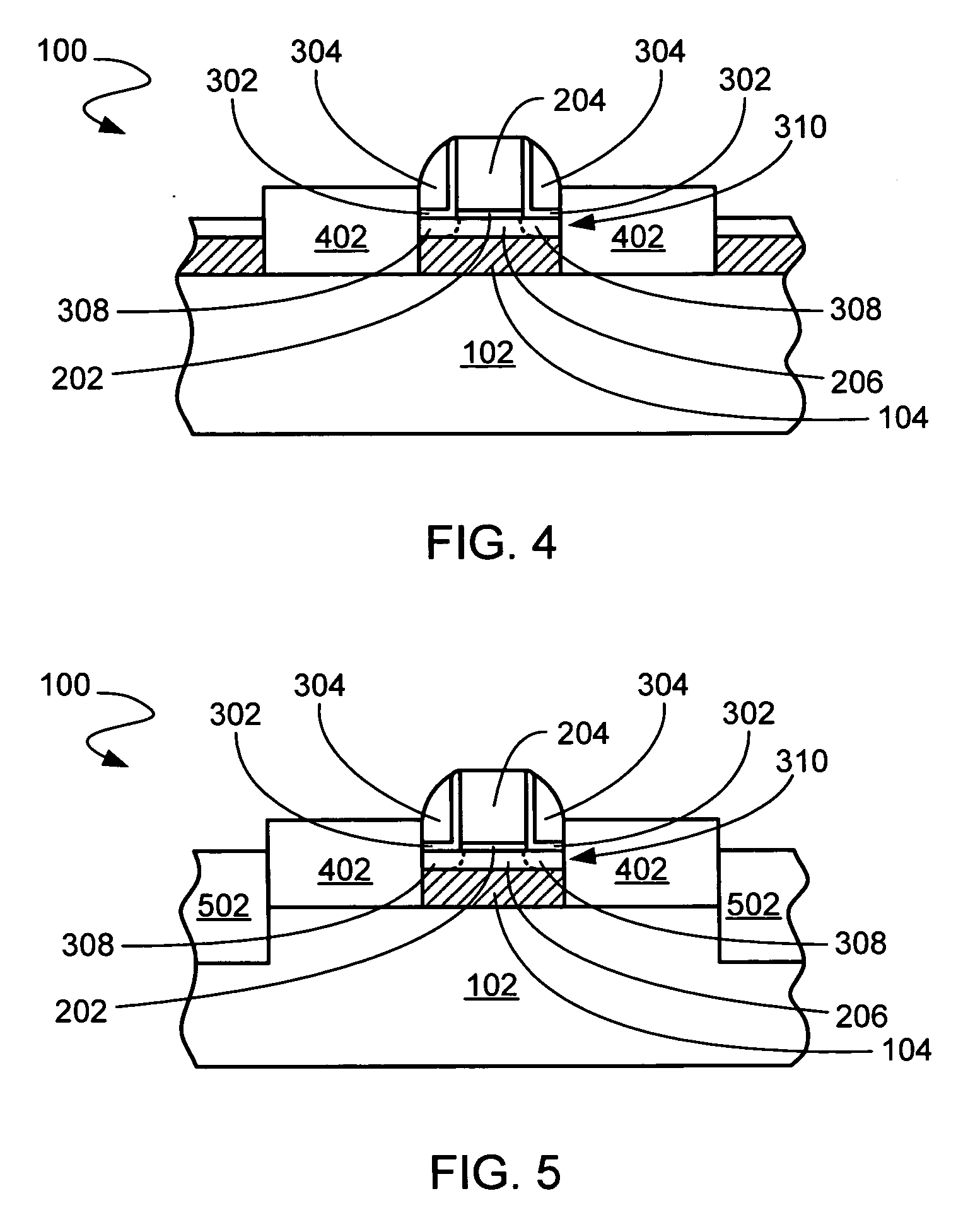
[0019]FIG. 4 shows the structure of FIG. 3 with recessed source / drain in accordance with an embodiment of the present invention;
[0020]FIG. 5 shows the structure of FIG. 4 after silicidation in accordance with an embodiment of the present invention;
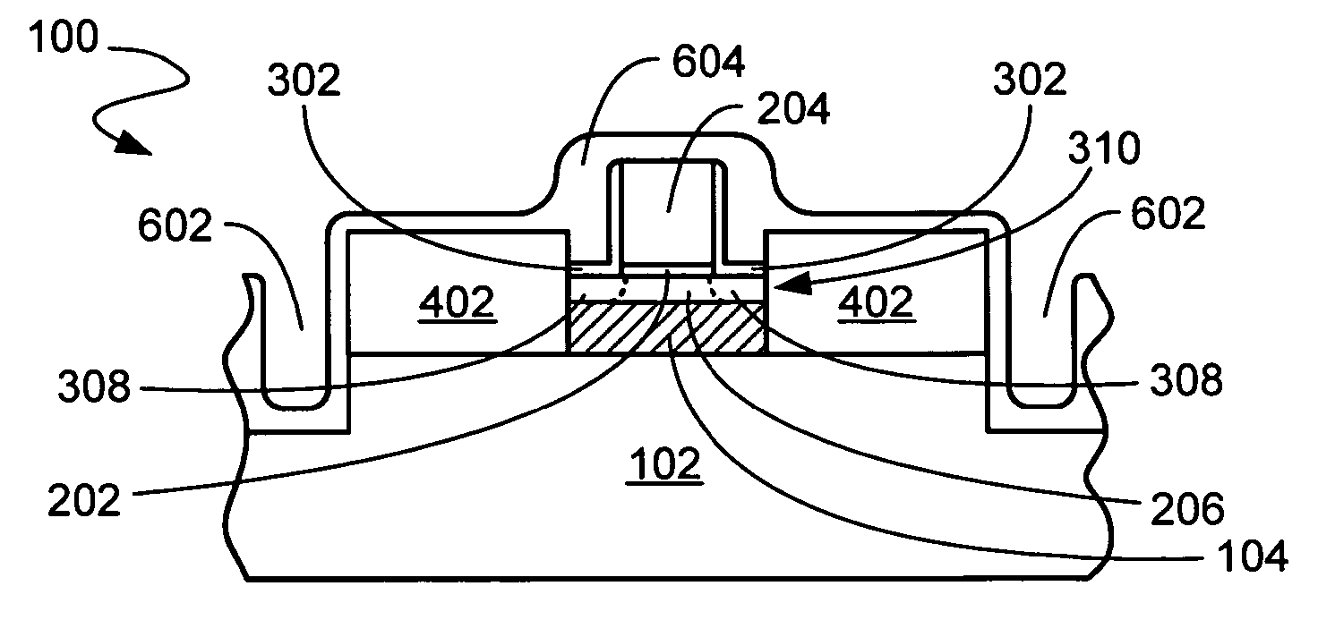
[0021]FIG. 6 shows the structure of FIG. 5 with a contact etch stop layer in accordance with an alternate embodiment of the present invention; and
[0023] In the following description, numerous specific details are given to provide a thorough understanding of the invention. However, it will be apparent that the invention may be practiced without these specific details. In order to avoid obscuring the present invention, some well-known device configurations and process steps are not disclosed in detail.
[0024] Likewise, the drawings showing embodiments of the device are semi-diagrammatic and not to scale and, particularly, some of the dimensions are for the
clarity of presentation and may be shown greatly exaggerated in the FIGs.
[0025] The term “horizontal” as used herein is defined as a
plane parallel to a substrate or wafer. The term “vertical” refers to a direction perpendicular to the horizontal as just defined. Terms, such as “on”, “above”, “below”, “bottom”, “top”, “side” (as in “sidewall”), “higher”, “lower”, “over”, and “under”, are defined with respect to the horizontal plane.
[0026] The term “
processing” as used herein includes deposition of material or
photoresist, patterning,
exposure, development,
etching, cleaning, and / or removal of the material or
photoresist as required in forming a described structure.
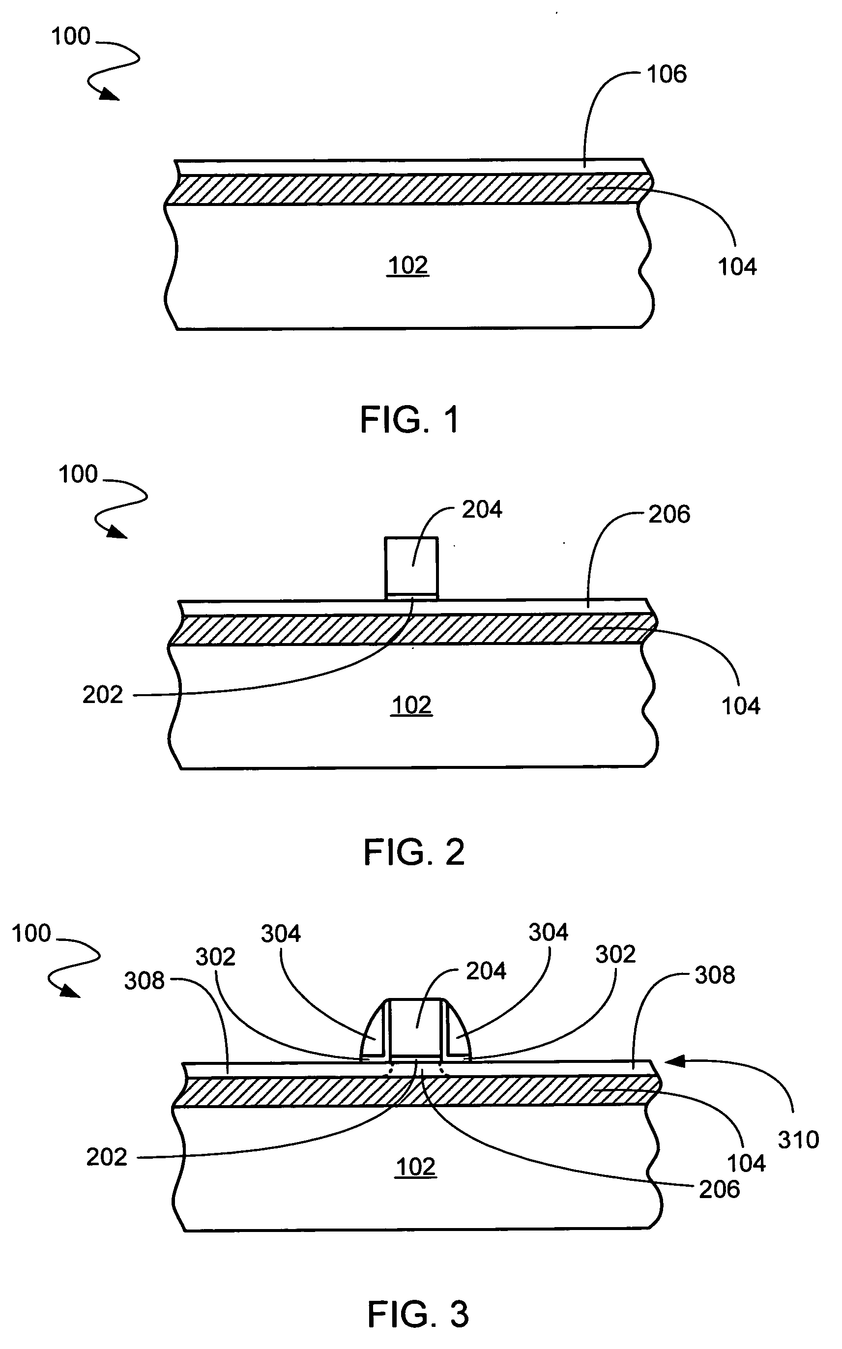
[0027] Referring now to FIG. 1, therein is shown a cross-section of a fully depleted
silicon on insulator (“FDSOI”) wafer 100, which includes a semiconductor substrate 102 of a material such as a p-doped silicon (“Si”). On top of the semiconductor substrate 102 is a
buried oxide layer (“BOX”) 104, which is an insulator layer of a material such as
silicon dioxide (“SiO2”), and a channel layer 106 of a
thin layer of Si.
[0028] In order to control short channel effects of 45 nm and below node with a 25 nm or smaller
gate length, it has been discovered that the channel layer 106 must be thinner than 100 Å in thickness.
[0029] A
deep trench isolation (“DTI”) 108, spaced outside recessed source / drain 402 (FIG. 4), has been added to the FDSOI wafer 100. The DTI 108 is formed with a
deep trench etch that etches through the channel layer 106, the BOX 104, and into the substrate 102. To maintain device isolation, the depth of the DTI must be greater than the recessed source / drain 402 (FIG. 4). In order to complete the DTI 108, the resulting deep trench is filled with a
dielectric of a material such as SiO2.
[0031] Referring now to FIG. 3, therein is shown the structure of FIG. 2 after further
processing. A recess etch of the DTI 108 prepares the wafer 100 for spacer formation in the DTI 108. A liner 302 of a material such as SiO2 is deposited on the gate 204, the channel layer 106, and the DTI 108. A spacer 304 of a material such as Si3N4 is formed around the gate portion of the liner 302 and in the DTI 108.
[0032] Among the
key issues for fabrication of FDSOI
CMOS is the formation of source and drain with low parasitic series resistance. One solution has been to elevate the source and drain. Elevated source and drain can be formed by selective epitaxial growth (“SEG”). Unfortunately, it is difficult to uniformly grow high quality, single crystalline source and drain on an extremely thin silicon island such as the channel layer 106. Furthermore, processes performed prior to SEG, such as oxidation, pre-clean, and H2 baking, can remove all or parts of the thin silicon needed for SEG.
[0033] Referring now to FIG. 4, therein is shown the structure of FIG. 3 after
processing in accordance with an embodiment of the present invention. Recessed source / drain 402 have been added to the FDSOI wafer 100. The channel layer 106 has been etched to form a channel 404.
[0034] To form the recessed source / drain 402, a suitable process, such as
etching, is used to penetrate through the channel layer 106 and the BOX 104 between the gate 204 and the DTI 108. It has been discovered that a thin BOX 104 from 100 Å-600 Å provides an optimal thickness. Selective epitaxial growth (“SEG”) then takes place on the surface of the substrate 102 and the sidewall of the channel 404. This ensures a continuous, high quality Si surface for the SEG of the recessed source / drain 402 even when silicon of the channel layer 106 may be partially or even entirely consumed by previous processes.
[0035] The resulting structure retains the advantages of elevated source and drain, such as low parasitic series resistance, while overcoming the problem of SEG on thin silicon. At this stage, performance can be improved through modification of the SEG of the recessed source / drain 402.
[0036] Referring now to FIG. 5, therein is shown the structure of FIG. 4 after further processing in accordance with an embodiment of the present invention. Silicidation takes place on the gate 204 and the source / drain 402 to form a NiSi layer 504.
[0037] It will be understood that the order of forming the recessed source / drain 402 and the DTI 108 is optional and the sequence described above has been done so as a matter of convenience. The recessed source / drain 402 can be formed in situ during selective epitaxial growth of the recessed source / drain 402 or by
ion implantation and rapid thermal anneal. Through strain engineered trench fill dielectrics, the DTI 108 introduces strain to the channel 404 and is preferred for isolation among transistors.
[0038] Introducing
tensile strain or compressive strain to the channels of FDSOI CMOS devices improves performance.
Tensile strain along the direction of current flow increases both
electron and hole mobility in an NMOS. On the other hand compressive strain improves performance of a PMOS by increasing hole mobility. Thus, applied strain as appropriate to the channel 404 significantly increases channel mobility, consequently increasing drive current by a significant fraction of the mobility
gain.

