Method and apparatus for rapid inline measurement of parameter spreads and defects in integrated circuit chips

a technology of in-line measurement and parameter spread, which is applied in the direction of semiconductor/solid-state device testing/measurement, instruments, testing circuits, etc., can solve the problems of affecting the yield and reliability of complementary metal oxide semiconductor products, test time and subsequently cost limitations preclude the measurement of a large array of field effect transistors (fets) in-line, and array failures do not directly provide information on individual mosfets

Inactive Publication Date: 2006-05-11
IBM CORP
View PDF4 Cites 27 Cited by
  • Summary
  • Abstract
  • Description
  • Claims
  • Application Information

AI Technical Summary

Problems solved by technology

Circuit failures, such as Static Random Access Memory (SRAM) cell instability fails in a large memory array, arising from statistical fluctuations in Metal-Oxide Semiconductor Field-Effect Transistor (MOSFET) parameters, or hard fails, from Back End of Line (BEOL) shorts and opens, directly impact both the yield and reliability of Complementary Metal Oxide Semiconductor (CMOS) products.
Test time and subsequently cost limitations preclude the measurements of a la

Method used


Image

  • Method and apparatus for rapid inline measurement of parameter spreads and defects in integrated circuit chips
  • Method and apparatus for rapid inline measurement of parameter spreads and defects in integrated circuit chips
  • Method and apparatus for rapid inline measurement of parameter spreads and defects in integrated circuit chips

Examples


Embodiment Construction

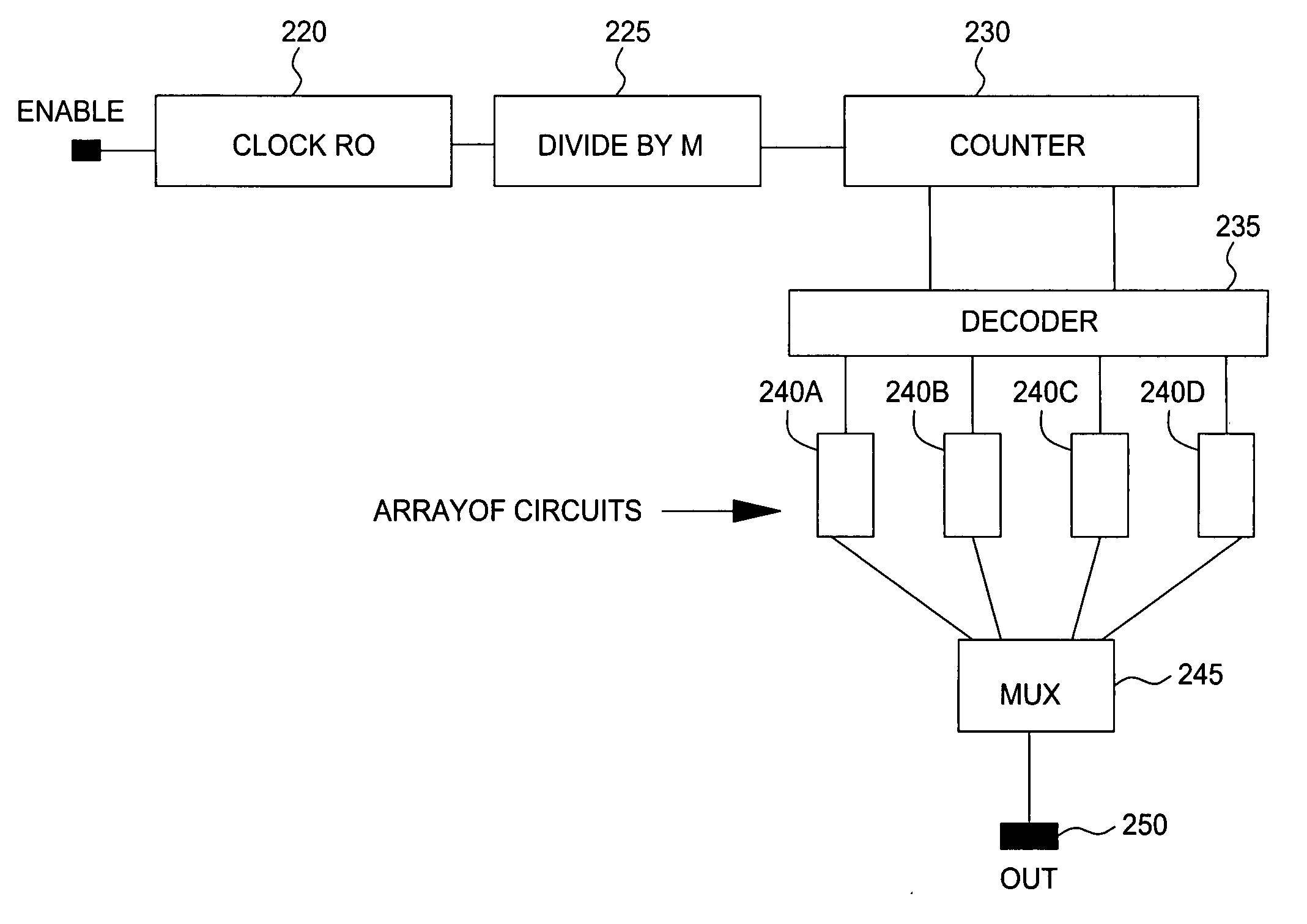
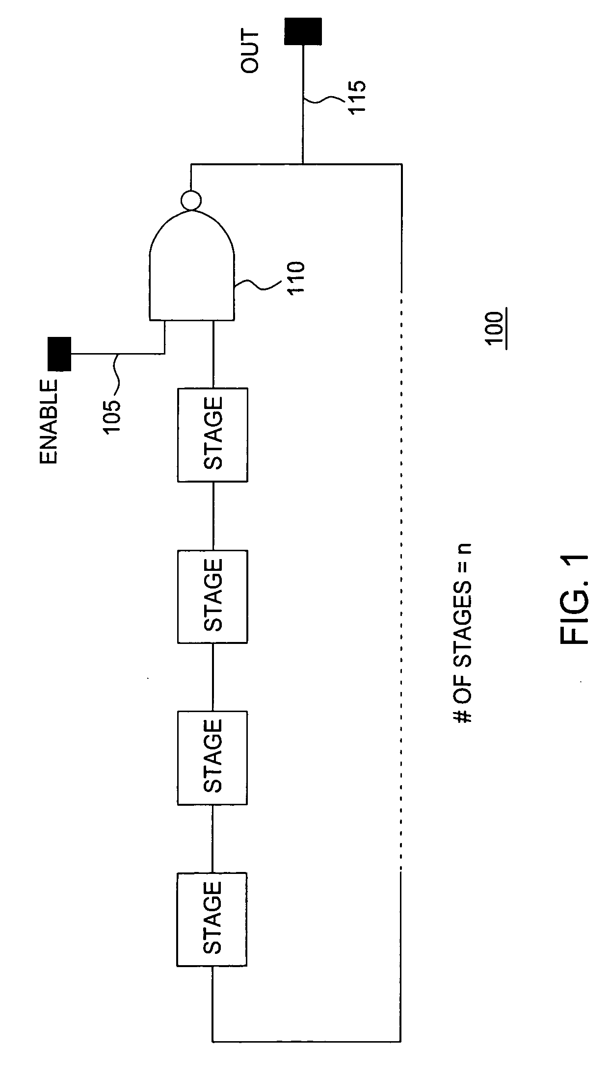
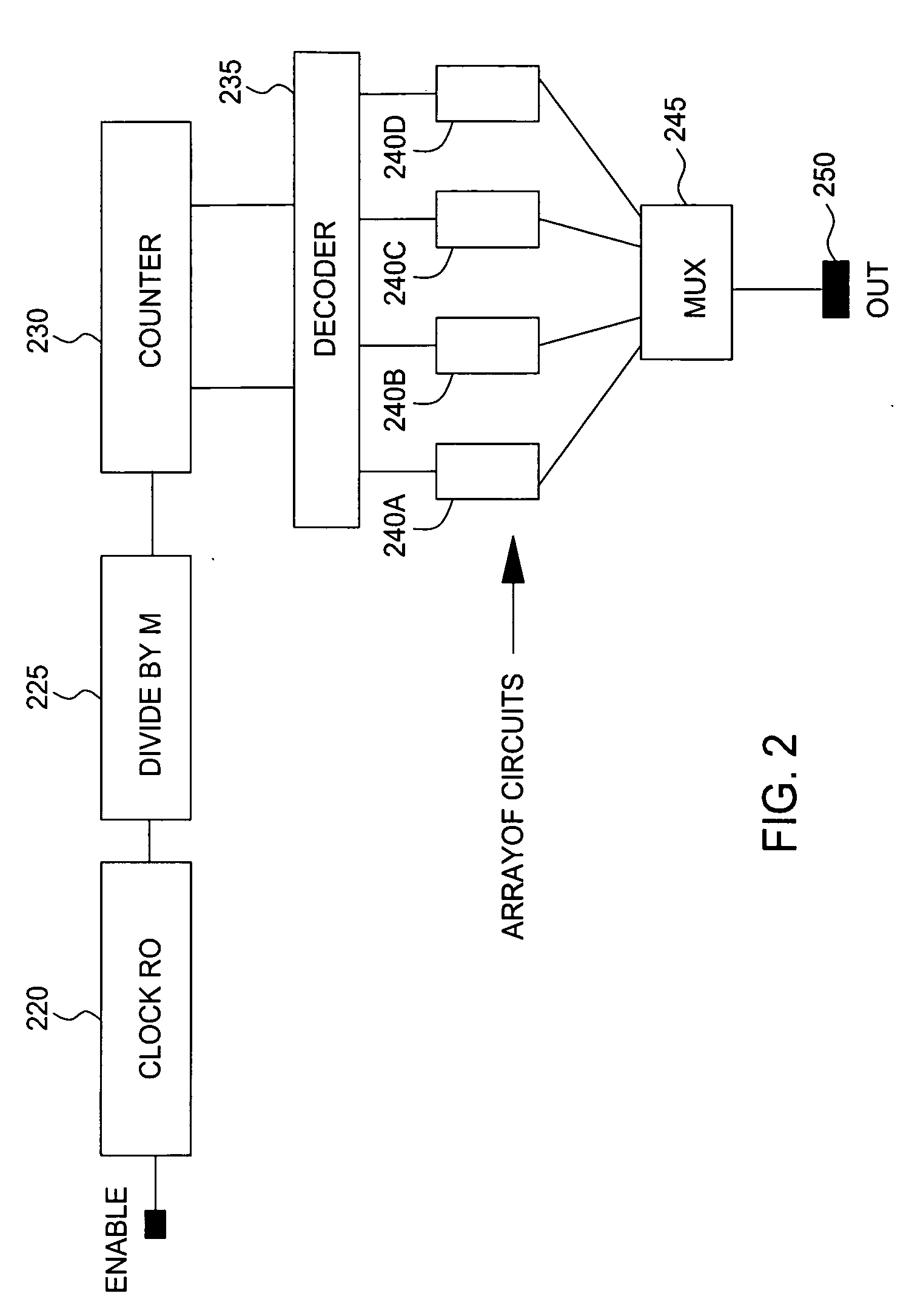
[0018] The circuit technique described in this disclosure allows rapid measurements of MOSFET characteristics (as well as random defects such as BEOL opens and shorts) by mapping parameter spreads, e.g., the variations in threshold voltage, to the variations in the output voltage, current, or frequency of an array of nominally identical semiconductor circuits. In other words, a distribution of an output signal, e.g., voltage current, frequency, would be used to gauge or determine the distribution of a parameter of interest, e.g., threshold voltage, drain current or drain to source current, current in a linear region of a transistor (e.g., n-channel FET or p-channel FET), or resistance. In one embodiment, the semiconductor circuits in the array are ring oscillators, with a common output, that are turned on and off sequentially. The output frequency of the array circuit is modulated as individual rings characterized by different values of Vt are selected, and a commercial frequency co...


PUM


Abstract

A method and apparatus for monitoring a plurality of semiconductor devices is disclosed. At least one array of 2n semiconductor circuits is provided. A clock ring oscillator provides a clock signal. The clock signal drives a frequency divider followed by an n-stage binary counter. The outputs from the counter's stages drive an n-input decoder which sequentially addresses each semiconductor circuit. An output signal from each semiconductor circuit is measured and read out over a common bus, where a distribution of the output signals is a measure of a distribution of a parameter of interest.

Description

BACKGROUND OF THE INVENTION [0001] Circuit failures, such as Static Random Access Memory (SRAM) cell instability fails in a large memory array, arising from statistical fluctuations in Metal-Oxide Semiconductor Field-Effect Transistor (MOSFET) parameters, or hard fails, from Back End of Line (BEOL) shorts and opens, directly impact both the yield and reliability of Complementary Metal Oxide Semiconductor (CMOS) products. MOSFET characteristics of a few devices (typically ten to twenty) are measured in the manufacturing line to monitor process variations, but provide little information on statistical variations. Test time and subsequently cost limitations preclude the measurements of a large array of field effect transistors (FETs) in-line. Process yield monitors use large memory arrays however array failures do not directly provide information on the individual MOSFET (Positive-Channel Metal Oxide Semiconductor (PMOS) and Negative-Channel Metal Oxide Semiconductor (NMOS)) components...

Claims


Application Information

Patent Timeline
IPC IPC(8): G06F19/00G01R27/28
CPCG01R31/31717G11C29/56G11C29/56012G11C2029/5602
Inventor BHUSHAN, MANJULKETCHEN, MARK B.
Owner IBM CORP
Why Eureka
Try Eureka