Post-etch treatment to remove residues

a post-etch treatment and residue technology, applied in the direction of cleaning process and apparatus, cleaning using gases, chemical instruments and processes, etc., can solve the problems of shrinking transistor size, affecting the performance of the device, and posing many challenges

Inactive Publication Date: 2006-05-18
APPLIED MATERIALS INC
View PDF99 Cites 36 Cited by
  • Summary
  • Abstract
  • Description
  • Claims
  • Application Information

AI Technical Summary

Benefits of technology

[0010] In another embodiment, a method of opening a dielectric barrier layer above a layer of copper lines on a semiconductor substrate during a damascene or dual damascene process is provided. The method includes introducing a fluorine-containing process gas into a vacuum chamber in which the substrate is located then maintaining a plasma of the fluorine-containing process gas in the vacuum chamber to etch the dielectric barrier layer, thereby uncovering surface of the layer of copper lines. A proce

Problems solved by technology

The continued shrinking of transistor sizes on the IC chips, however, poses many challenges to backend interconnects.
As the minimum feature size on the IC's shrinks below 0.18 μm, the metal interconnect lines become thinner and more densely packed, resulting in greater resistance in the metal lines and larger intermetal capacitance, and therefore a

Method used


Image

  • Post-etch treatment to remove residues
  • Post-etch treatment to remove residues
  • Post-etch treatment to remove residues

Examples


example

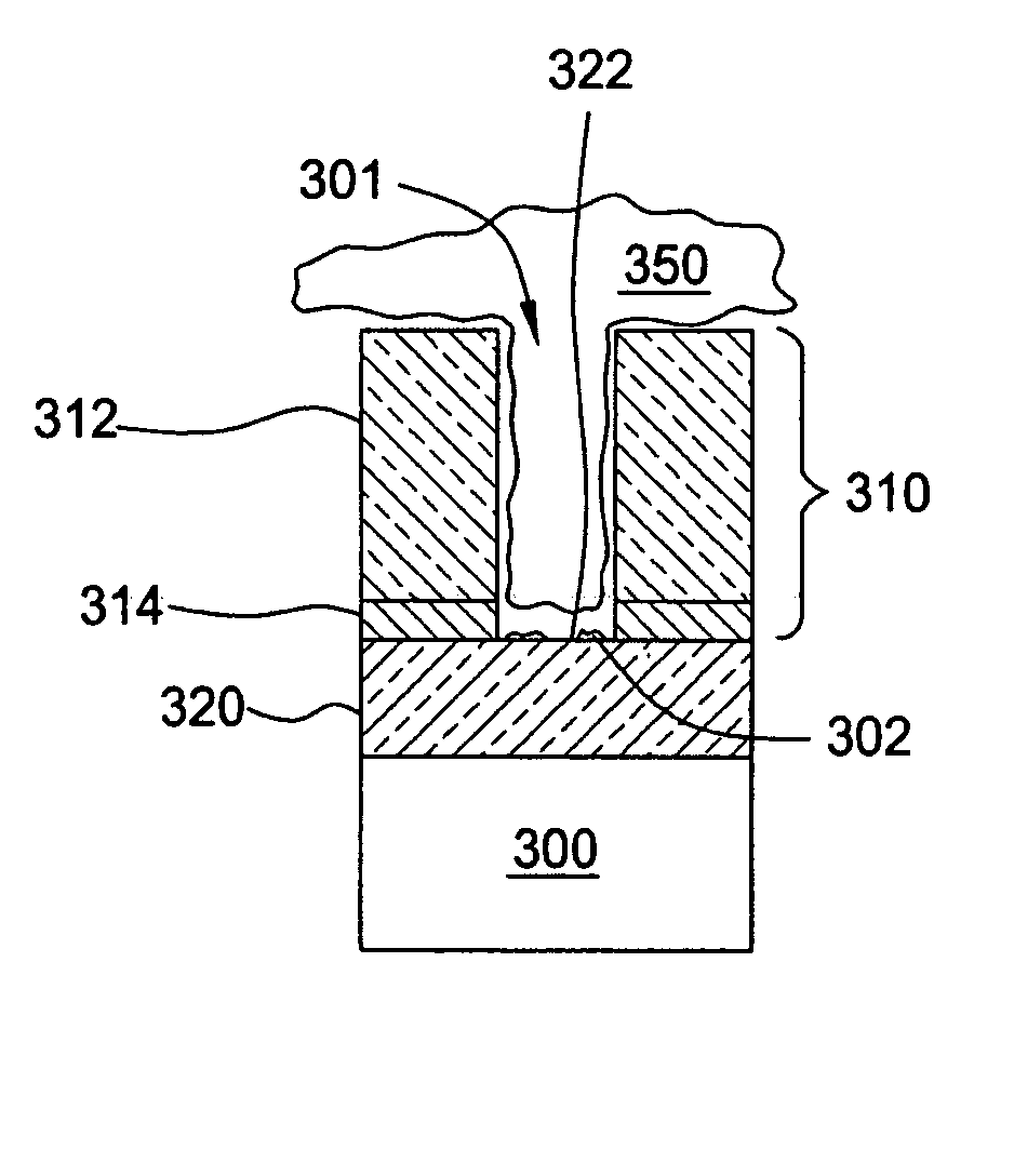
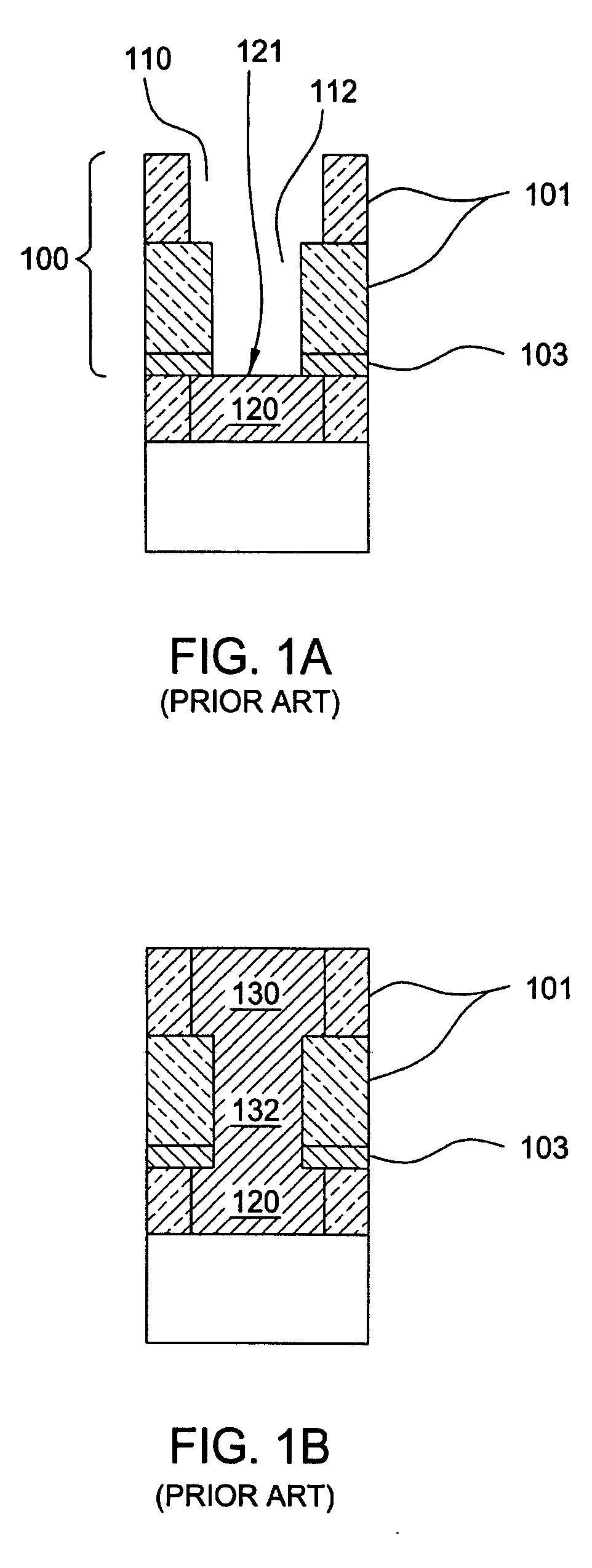
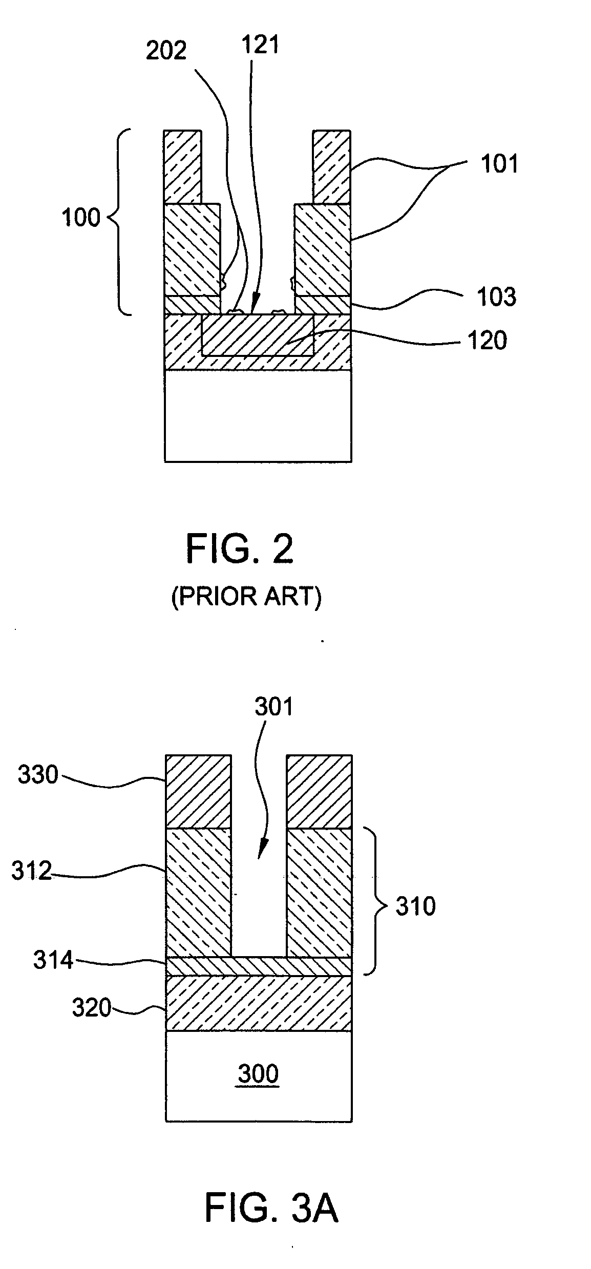
[0041] To illustrate applications of the present invention, the substrate 300 with layers of materials formed thereon as shown in FIG. 3B or 5E is prepared according to the process flow described in steps 402 through 404, shown in FIG. 4, or steps 602 through 610, shown in FIG. 6. In one embodiment, the substrate 300 may be a silicon substrate of 200 mm (8 inch) or 300 mm (12 inch) diameter. The low-k dielectric layer 312 may have a thickness of about 0.4-1.5 microns. The barrier layer 314 may have a thickness of about a few hundred angstroms. One example of a material suitable for use as the low-k dielectric layer 312 in FIG. 3B or 5E is Black Diamond™ film, commercially available from Applied Materials, Inc., of Santa Clara, Calif. One example of a material suitable for use as the low-k dielectric barrier layer 314 is BLOk™ (barrier low-k) film, also available from Applied Materials. BLOk™ film is a silicon carbide based film formed using the chemical vapor deposition (CVD) or pla...


PUM

PropertyMeasurementUnit
Temperatureaaaaaaaaaa

Abstract

A method for removing residue from a layer of conductive material on a substrate is provided herein. In one embodiment, the method includes introducing a process gas into a vacuum chamber having a substrate surface with residue from exposure to a fluorine-containing environment. The process gas includes a hydrogen-containing gas. Optionally, the process gas may further include an oxygen-containing or a nitrogen containing gas. A plasma of the process gas is thereafter maintained in the vacuum chamber for a predetermined period of time to remove the residue from the surface. The temperature of the substrate is maintained at a temperature between about 10 degrees Celsius and about 90 degrees Celsius during the plasma step.

Description

BACKGROUND OF THE INVENTION [0001] 1. Field of the Invention [0002] The present invention relates to semiconductor processing technologies and, more particularly, to treating post-etch material surfaces to remove residues. [0003] 2. Description of the Related Art [0004] The performance, density, and cost of integrated circuit (IC) chips have been improving at a dramatic rate. Much of the improvement has been due to the ability to scale transistors to increasingly smaller dimensions, resulting in higher speed and higher functional density. The continued shrinking of transistor sizes on the IC chips, however, poses many challenges to backend interconnects. As the minimum feature size on the IC's shrinks below 0.18 μm, the metal interconnect lines become thinner and more densely packed, resulting in greater resistance in the metal lines and larger intermetal capacitance, and therefore a longer time delay or slower operating speed. By changing to different materials, such as higher cond...

Claims


Application Information

Patent Timeline
IPC IPC(8): B08B6/00B08B5/04
CPCB08B7/00C23F4/00H01L21/02063H01L21/31116H01L21/76808H01L21/76814H01L21/304H01L21/3065
Inventor CHIANG, KANG-LIECAI, MAN-PINGMA, SHAWMINGYE, YANHSIEH, PETER
Owner APPLIED MATERIALS INC
Why Eureka
Try Eureka