Precursor compositions for forming tantalum-containing films, and tantalum-containing barrier films and copper-metallized semiconductor device structures

a technology of barrier films and precursor compositions, which is applied in the direction of thermoelectric devices, semiconductor/solid-state device details, group 5/15 element organic compounds, etc., can solve the problems of nitrogen photoresist poisoning, always problematic thermal stability of precursors,

Inactive Publication Date: 2006-05-18
ADVANCED TECH MATERIALS INC
View PDF49 Cites 34 Cited by
  • Summary
  • Abstract
  • Description
  • Claims
  • Application Information

AI Technical Summary

Benefits of technology

[0020] Other aspects, features and advantages of the invention will b

Problems solved by technology

Thermal stability is always problematic for such precursors.
This practice has a significant drawback in that it involves the presence of active nitrogen species deriving from the precursor and/or reactive gas environment in the deposition

Method used


Image

  • Precursor compositions for forming tantalum-containing films, and tantalum-containing barrier films and copper-metallized semiconductor device structures
  • Precursor compositions for forming tantalum-containing films, and tantalum-containing barrier films and copper-metallized semiconductor device structures
  • Precursor compositions for forming tantalum-containing films, and tantalum-containing barrier films and copper-metallized semiconductor device structures

Examples


Embodiment Construction

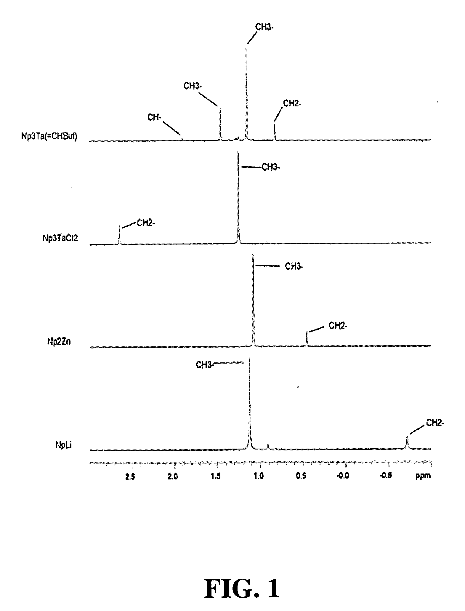
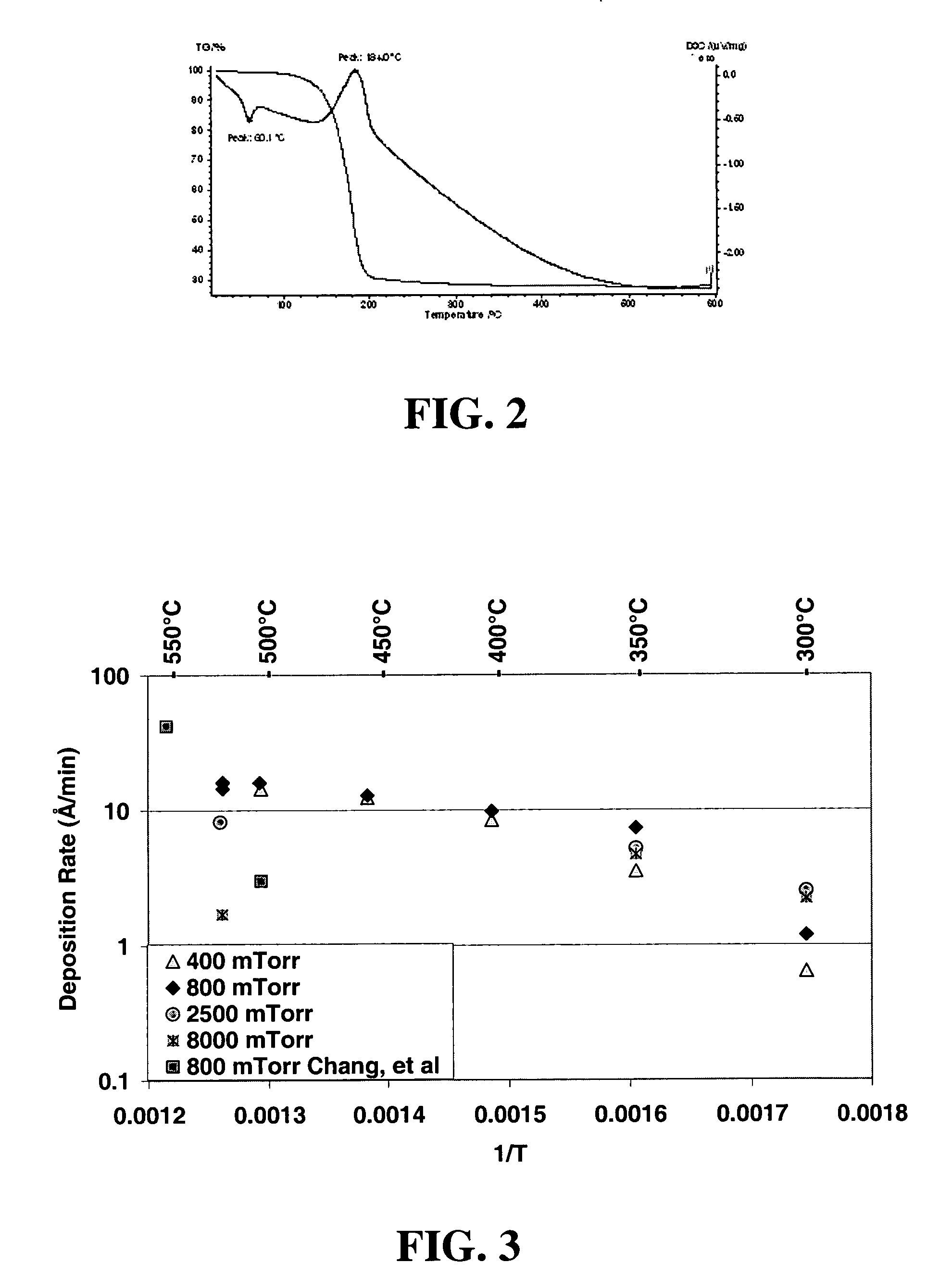
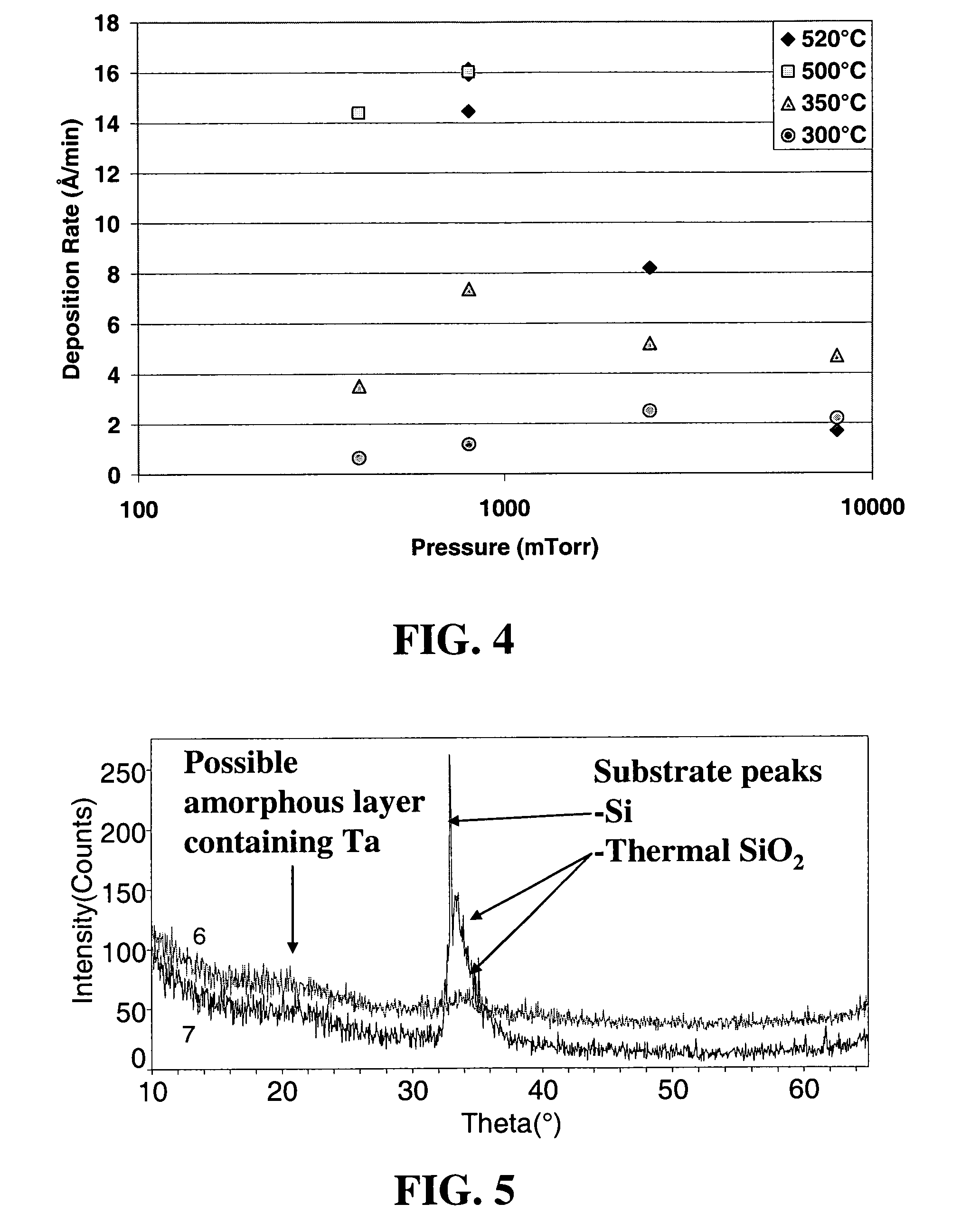
[0027] The present invention relates in various aspects to precursor compositions useful for forming tantalum-containing films, as well as to tantalum-containing films, such as may be employed as barrier layers in semiconductor devices utilizing copper metallization, as well as to semiconductor device structures including tantalum-containing films.

[0028] As used herein, the term “semiconductor device structures” is intended to be broadly construed to include microelectronic devices, products, components, assemblies and subassemblies that include a semiconductor material as a functional material therein. Illustrative examples of semiconductor device structures include, without limitation, resist-coated semiconductor substrates, flat-panel displays, thin-film recording heads, microelectromechanical systems (MEMS), and other advanced microelectronic components. The semiconductor device structure may include patterned and / or blanketed silicon wafers, flat-panel display substrates or fl...


PUM

PropertyMeasurementUnit
Temperatureaaaaaaaaaa

Abstract

Tantalum compositions of Formulae I-V hereof are disclosed, having utility as precursors for forming tantalum-containing films. The tantalum compositions are amenable to usage involving chemical vapor deposition and atomic layer deposition processes, to form semiconductor device structures, including a dielectric layer, a barrier layer overlying the dielectric layer, and copper metallization overlying the barrier layer, wherein the barrier layer includes a Ta-containing layer including sufficient carbon so that the Ta-containing layer is amorphous. In one preferred implementation, the semiconductor device structure is fabricated by depositing the Ta-containing barrier layer, via CVD or ALD, from a precursor including a Ta alkylidene compound, at a temperature below 400° C., in a reducing or inert atmosphere.

Description

CROSS-REFERENCE TO RELATED APPLICATIONS [0001] The benefit of U.S. Provisional Patent Application No. 60 / 628,422 filed Nov. 16, 2004 and of U.S. Provisional Patent Application No. 60 / 636,284 filed Dec. 15, 2004 is hereby claimed under the provisions of 35 USC 119. The disclosures of said provisional applications are hereby incorporated by reference herein, for all purposes.FIELD OF THE INVENTION [0002] The present invention relates to precursor compositions that are useful for forming tantalum-containing films, e.g., by chemical vapor deposition (CVD) or atomic layer deposition (ALD), as well as to tantalum-containing barrier films and to copper-metallized semiconductor device structures including tantalum-containing films. DESCRIPTION OF THE RELATED ART [0003] In the field of semiconductor manufacturing, copper (Cu) and low k dielectrics are being increasingly employed in high performance silicon integrated circuits. Since Cu is very mobile in silicon (Si) and silicon dioxide (SiO2...

Claims


Application Information

Patent Timeline
IPC IPC(8): H01L29/08C07F9/00C07F17/00H01L21/469
CPCC07F9/00C07F9/005C07F17/00C23C16/18C23C16/34H01L21/28556H01L21/28562H01L21/76843H01L23/53238H01L2924/0002H01L2924/00
Inventor HENDRIX, BRYAN C.ROEDER, JEFFREY F.BAUM, THOMAS H.CHEN, TIANNIUXU, CHONGYINGSTAUF, GREGORY T.
Owner ADVANCED TECH MATERIALS INC
Why Eureka
Try Eureka