Semiconductor device, manufacturing method of the same, and electronic device

Inactive Publication Date: 2006-05-25
RENESAS TECH CORP
View PDF2 Cites 30 Cited by
  • Summary
  • Abstract
  • Description
  • Claims
  • Application Information

AI Technical Summary

Benefits of technology

[0014] An effect obtained by the representative one of the inventions disclosed in the application will be briefly described as follows.
[0015] By optimizing the lower limi

Problems solved by technology

When the HBT 51 is operated by energizing, the temperature of the emitter electrode 53 rises locally (in particular, the regions surrounded by relatively-thick alternate long and short dash lines), the characteristic deterioration is accelerated, and a problem occurs such that the life of the HBT 51 at the time of operation (energizing) test is shortened.
However, since the thermal conductivity of WSi

Method used


Image

  • Semiconductor device, manufacturing method of the same, and electronic device
  • Semiconductor device, manufacturing method of the same, and electronic device
  • Semiconductor device, manufacturing method of the same, and electronic device

Examples


first embodiment

[0046] An example of a semiconductor device including a hetero-junction bipolar transistor (HBT) as a first embodiment will be described by referring to FIGS. 1 to 25. Briefly, the structure of an HBT in the embodiment will be described first with reference to FIGS. 1 to 11 and, after that, a method of manufacturing a semiconductor device including the HBT will be described with reference to FIGS. 12 to 25.

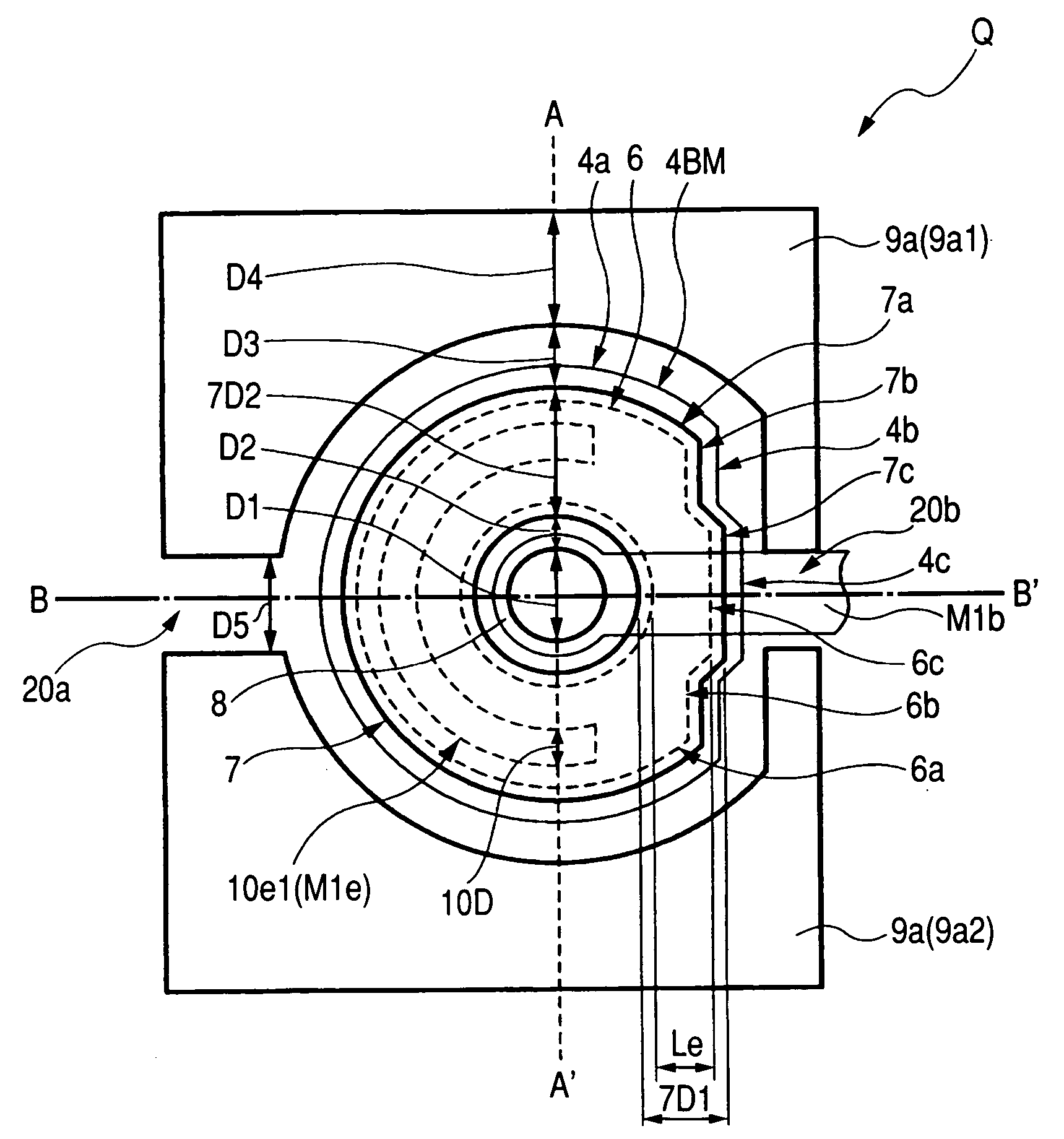
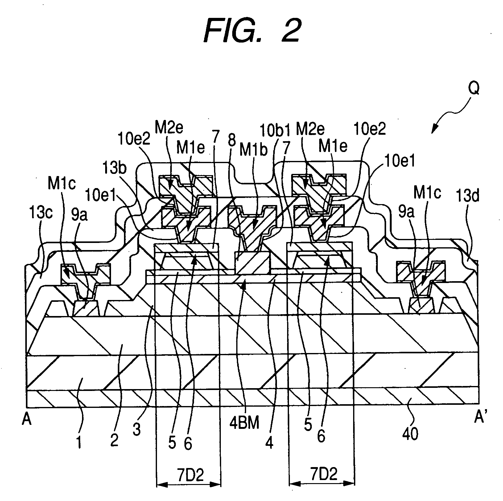
[0047] First, the structure of a semiconductor device including an HBT of the embodiment will be described. FIG. 1 is a plan view showing an example of an HBT(Q) of the embodiment and shows a layout of a base electrode 8, an emitter electrode 7, a collector electrode 9a, a base mesa 4BM, an emitter contact layer 6, a contact hole 10e1, and a base lead line M1b of an HBT(Q) formed on a substrate. The layout is in a plane parallel with the main surface of the substrate where the HBT(Q) is formed.

[0048] As shown in FIG. 1, in the HBT(Q), the base electrode 8 is disposed, the emitte...

second embodiment

[0108] In a second embodiment, an example of an electronic device including a power amplifier having one or a plurality of hetero-junction bipolar transistors (HBTs) in the first embodiment will be described by using a power amplifier module with reference to FIGS. 26 to 28. FIG. 26 is a plan view of a main part of a power amplifier module PAM of the second embodiment. FIG. 27 is a plan view of a main part of a semiconductor chip (hereinbelow, simply called the chip) constructing the power amplifier module PAM. FIG. 28 is a circuit diagram of a main part of the power amplifier module PAM.

[0109] The power amplifier module PAM of the second embodiment has an operating frequency of about 500 MHz or higher and is a power amplifier module PAM of the GSM (Global System for Mobile Communication) in which the operating frequency is about 800 MHz to 900 MHz, the DCS (Digital Cellular System) in which the operating frequency is about 1.8 GHz to 1.9 GHz), or a system corresponding to both of ...


PUM


Abstract

The invention is directed to improve characteristics of an HBT (Hetero-junction Bipolar Transistor). An HBT has a collector layer, a base layer, and an emitter layer formed in order on a main surface of a substrate made of a compound semiconductor and a collector electrode, a base electrode, and an emitter electrode electrically connected to the collector layer, the base layer, and the emitter layer, respectively, and further has an emitter contact layer formed between the emitter electrode and the emitter layer. The plane shape of the emitter contact layer and the emitter electrode is an almost annular shape surrounding the base electrode in a plane parallel with the main surface of the substrate, and the lower limit of the emitter contact layer is 1.2 μm or larger.

Description

CROSS-REFERENCE TO RELATED APPLICATION [0001] The present application claims priority from Japanese patent application No 2004-337198 filed on Nov. 22, 2004, the content of which is hereby incorporated by reference into this application. BACKGROUND OF THE INVENTION [0002] The present invention relates to a semiconductor device and a technique of manufacturing the same. More particularly, the invention relates to a technique effective when applied to a hetero-junction bipolar transistor (hereinbelow, called HBT) and to an electronic device using the same HBT. [0003] As one of bipolar transistors in each of which a collector layer, a base layer, and an emitter layer are sequentially formed on a substrate (semiconductor substrate) made of a compound semiconductor such as GaAs, a mesa transistor (mesa junction bipolar transistor) having a trapezoidal shape in cross section and whose surface in which an emitter and a base are formed is smaller than that of the substrate is known. Since a...

Claims


Application Information

Patent Timeline
IPC IPC(8): H01L31/11H01L27/082
CPCH01L27/0605H01L29/0692H01L29/7371H03F3/19
Inventor KUROKAWA, ATSUSHIUMEMOTO, YASUNARISASAKI, SATOSHI
Owner RENESAS TECH CORP
Why Eureka
Try Eureka