Semiconductor device and layout design method for the same

Inactive Publication Date: 2006-06-01
PANASONIC CORP
View PDF0 Cites 66 Cited by
  • Summary
  • Abstract
  • Description
  • Claims
  • Application Information

AI Technical Summary

Benefits of technology

[0017] Specifically, according to the present invention, portions of a gate interconnect having a larger dimension along the gate length direction than a gate electrode are laid out to be symmetrical with respect to a device forming region. Therefore, even when the gate flaring or the alignment shift between the GA/OD photomasks occurs, transistors whose arrangement directions are different from each other by 180° can be the same in the shape of their gate electrodes. Accordingly, variation in the gate l

Problems solved by technology

The optical proximity effect is, however, unavoidable in principle, and therefore, it is difficult to avoid the optical proximity effect merely by the fabrication/process technique such as the super-resolutio

Method used


Image

  • Semiconductor device and layout design method for the same
  • Semiconductor device and layout design method for the same
  • Semiconductor device and layout design method for the same

Examples


embodiment 1

[0031] Now, a semiconductor device according to Embodiment 1 and a layout design method for the same will be described with reference to the accompanying drawings.

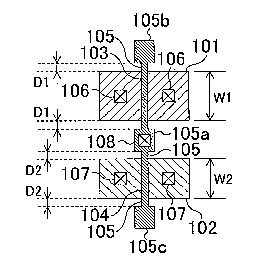
[0032]FIG. 1A is a plan view of a design shape of the semiconductor device of Embodiment 1 and FIGS. 1B through 1D are plan views of fabricated shapes of the semiconductor device of Embodiment 1.

[0033] As shown in FIG. 1A, a P-type impurity diffusion region 101 and an N-type impurity diffusion region 102 each surrounded with an isolation region (not shown) of STI (shallow trench isolation) or the like are formed on a semiconductor substrate (not shown) to be adjacent to each other. A conductive pattern (of, for example, a gate polysilicon film) corresponding to a gate electrode 103 and a gate electrode 104 is formed on the P-type impurity diffusion region 101 and the N-type impurity diffusion region 102, and the conductive pattern extends over the isolation region disposed on the both sides of the impurity diffusion regi...

modification 1

of Embodiment 1

[0044] Now, a semiconductor device according to Modification 1 of Embodiment 1 and a layout design method for the same will be described with reference to the accompanying drawings.

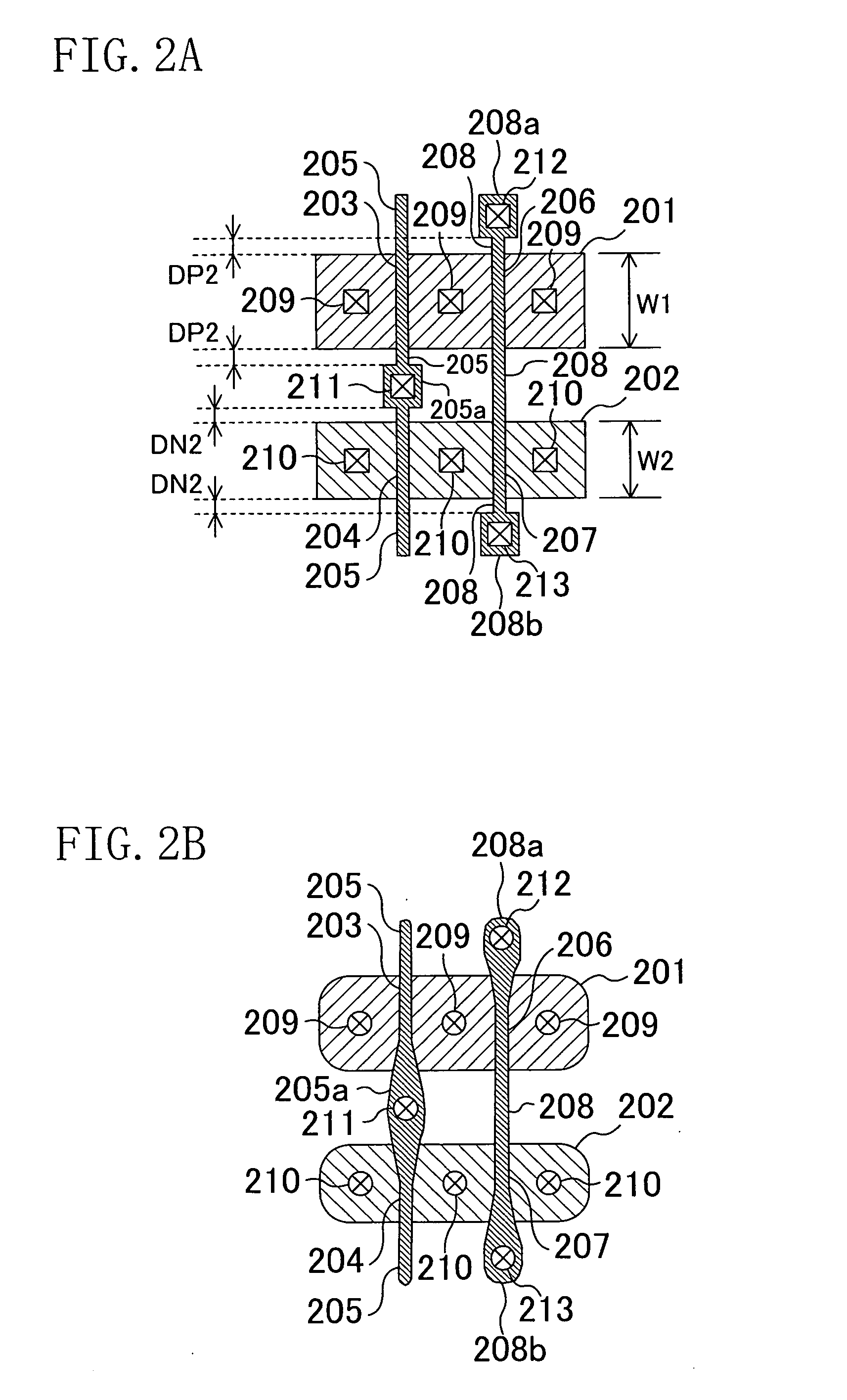
[0045]FIG. 2A is a plan view of a design shape of the semiconductor device of Modification I of Embodiment 1 and FIG. 2B is a plan view of a fabricated shape of the semiconductor device of Modification 1 of Embodiment 1.

[0046] As shown in FIG. 2A, a P-type impurity diffusion region 201 and an N-type impurity diffusion region 202 each surrounded with an isolation region (not shown) of STI or the like are formed on a semiconductor substrate (not shown) to be adjacent to each other. A first conductive pattern (of, for example, a gate polysilicon film) corresponding to a gate electrode 203 and a gate electrode 204 and a second conductive pattern (of, for example, a gate polysilicon film) corresponding to a gate electrode 206 and a gate electrode 207 are formed on the P-type impurity diffusion...

modification 2

of Embodiment 2

[0100] Now, a semiconductor device according to Modification b 2 of Embodiment 2 and a layout design method for the same will be described with reference to the accompanying drawing.

[0101]FIG. 7 is a plan view of a shape of a pattern actually formed on a semiconductor substrate when the semiconductor device having the design shape of FIG. 5A is fabricated through given semiconductor device fabrication process. In FIG. 7, like reference numerals are used to refer to like elements used in the semiconductor device shown in FIG. 5A so as to omit the description.

[0102] Specifically, in this modification, at the stage of transistor design, the distance between the portion of the gate interconnect 503 having the larger dimension along the gate length direction than the gate electrode 502 and the impurity diffusion region 501 is set to be not larger than a value obtained by subtracting the maximum value Dma of the GA / OD photomask alignment shift from the thickness Dsw of th...


PUM


Abstract

In layout design of a semiconductor device including a device forming region formed on a substrate; an isolation region formed on the semiconductor substrate so as to surround the device forming region; a gate electrode formed on the device forming region; and a gate interconnect connected to the gate electrode and formed on both sides of the device forming region on the isolation region, the semiconductor device is designed as follows: The gate interconnect has a first portion with a larger dimension along the gate length direction than the gate electrode on one side of the device forming region and has a second portion with a larger dimension along the gate length direction than the gate electrode on the other side of the device forming region; and a distance between the first portion and the device forming region is equal to a distance between the second portion and the device forming region.

Description

CROSS-REFERENCE TO RELATED APPLICATIONS [0001] This application claims priority under 35 U.S.C. §119 on Patent Application No. 2004-346356 filed in Japan on Nov. 30, 2004, the entire contents of which are hereby incorporated by reference.BACKGROUND OF THE INVENTION [0002] The present invention relates to a semiconductor device including a refined transistor, and more particularly, it relates to countermeasure against dimensional variation caused by a mask alignment shift or an optical proximity effect in fabrication process for semiconductor devices. [0003] Principal factors for causing variation in propagation delay time in design of a semiconductor integrated circuit (LSI) are an operation power voltage, a temperature, process variation and the like. Also, in LSI design, the operation of an LSI should be guaranteed even when all the conditions are the worst. A gate length and a gate width of a transistor are significant elements for defining the operation of the transistor, and in...

Claims


Application Information

Patent Timeline
IPC IPC(8): H01L23/58
CPCH01L23/4824H01L27/0211H01L2924/0002H01L2924/00
Inventor TAMAKI, YASUHIROYAMASHITA, KYOJIOTANI, KATSUHIRO
Owner PANASONIC CORP
Why Eureka
Try Eureka