Tunneling diode logic IC using CML-type input driving circuit configuration and monostable bistable transition logic element (MOBILE)

a logic element and diode logic technology, applied in the field of high-speed logic gates, can solve the problems of limiting the operation speed of the circuit and increasing power consumption, and achieve the effects of reducing complexity of the circuit, improving overall speed of the circuit, and improving compatibility with existing logic gates

Inactive Publication Date: 2006-06-22
KOREA ADVANCED INST OF SCI & TECH
View PDF4 Cites 5 Cited by
  • Summary
  • Abstract
  • Description
  • Claims
  • Application Information

AI Technical Summary

Benefits of technology

[0024] As described in the above, the present invention provides a plurality of advantages for digital logic gates. The advantageous effects are as follows.
[0025] 1) The problem related to the adjustment of input voltage, which was a problem in existing MOBILE, is resolved. The previously described problem(if voltage is not accurately adjusted, operation of flip-flop fails) occurs in prior arts owing to abrupt increment of the current flows at a-transistor(115) in accordance with the increment of input voltage. However, in the present invention, the maximum current heading out from output port to input driving circuit is decided as lee by using CML gate. Thus, it is not necessary to adapt accurately input voltage to unintentional device characteristics, as is in existing MOBILE method.
[0026] 2) By utilizing CML gate as input driving circuit, compatibility with existing logic gates(CML, ECL, SCFL, etc.) is improved. The logic circuit sequentially processing signals can be configured by being able to apply the output of logic circuit to the input of the next stage logic circuit without additional devices by adjusting reference voltage(Vref).
[0027] 3) Since transistors of CML gate operate in bias condition operating at maximum speed, the overall speed of the circuit is improved.
[0028] 4) A plurality of functions can be implemented by using the switching characteristics of CML gate. That is, by exchanging input ports, inverted return-to-zero D flip-flop and non-inverted return-to-zero D flip-flop can be implemented. Return-to-zero OR gate and return-to-zero NOR gate can be implemented with an additional transistor.
[0029] 5) By connecting same series tunneling circuits to the input ports, differential voltage can be obtained simultaneously from a single input, thereby the complexity of the circuit can be reduced and the compatibility with existing circuits (ECL, SCFL, CML) can be improved.

Problems solved by technology

Since however these technologies use feedback loop, circuit configuration is complex and the number of the device count is large, thereby have disadvantages of limiting operational speed of circuit and increasing power consumption.

Method used


Image

  • Tunneling diode logic IC using CML-type input driving circuit configuration and monostable bistable transition logic element (MOBILE)
  • Tunneling diode logic IC using CML-type input driving circuit configuration and monostable bistable transition logic element (MOBILE)
  • Tunneling diode logic IC using CML-type input driving circuit configuration and monostable bistable transition logic element (MOBILE)

Examples


Embodiment Construction

[0062] Hereinafter, referring to appended drawings, the structures and operation principles for the embodiments of present invention are described in detail.

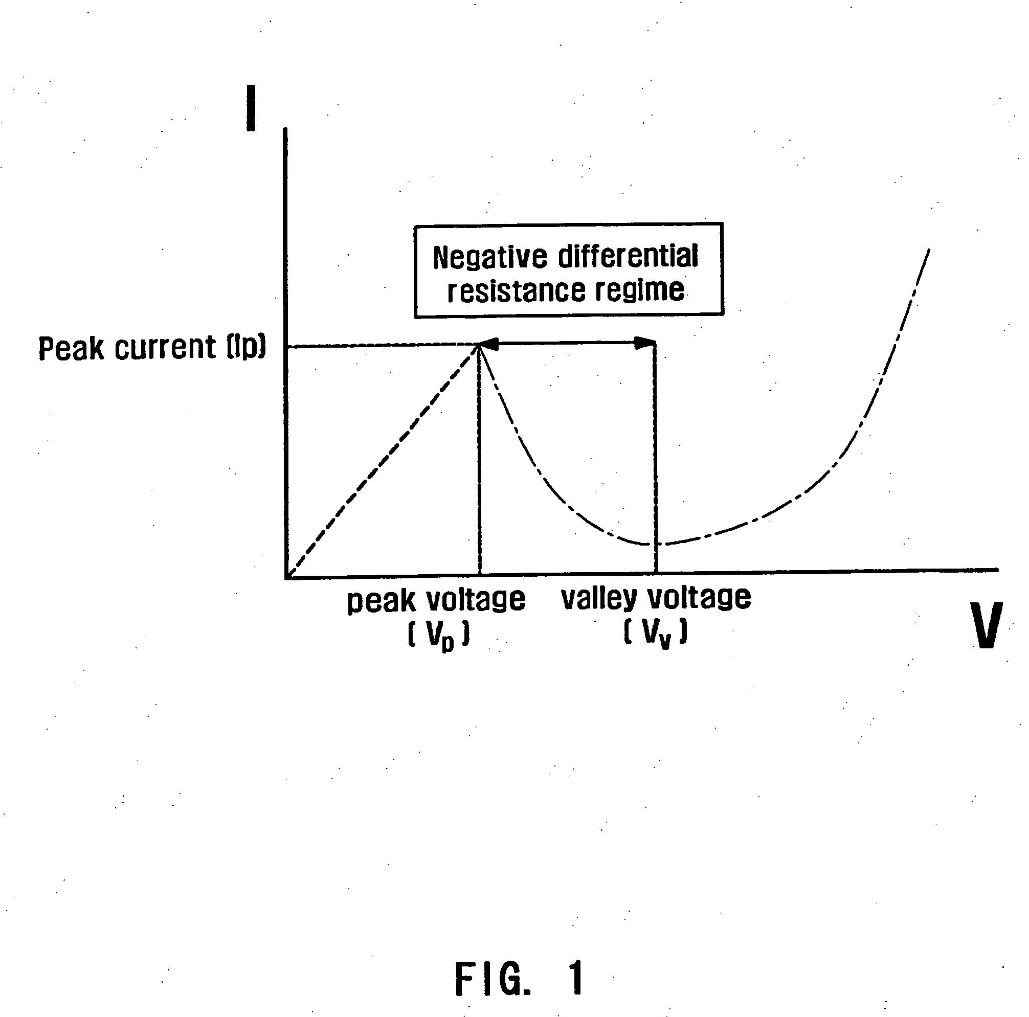
[0063] The present invention can be applied to basic technologies of all the 3-terminal switching devices including BJT and FET, which hereinafter, will be explained with the basis of high-speed HBT among BJT. The present invention can also be applied to all the tunneling diode technologies, which hereinafter, will be explained with the basis of InP based RTD having low peak voltage(Vp) and high PVCR(peak to valley current ratio).

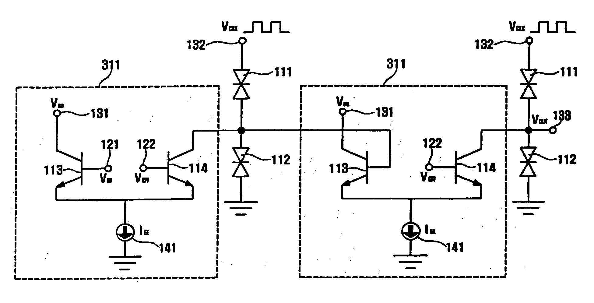
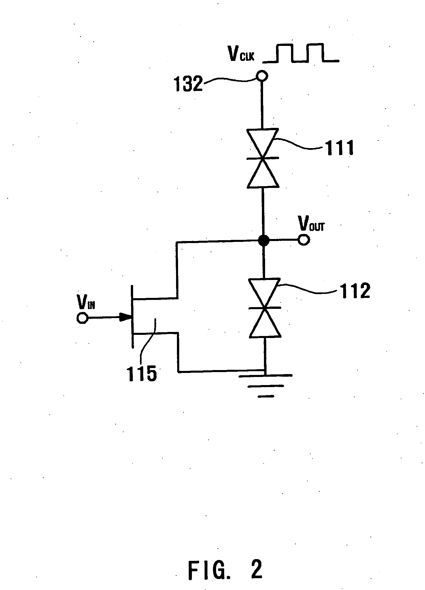
[0064]FIG. 6 is a circuit configuration diagram for a non-inverted return-to-zero D flip-flop configured with RTD logic gate using CML-type input driving circuit configuration and MOBILE proposed in the present invention. As shown in FIG. 6, two tunneling diodes are connected in a series. Driver RTD(112) is connected to ground and load RTD(1111) is connected to clock voltage port(132). A rectangular o...


PUM


Abstract

The present invention relates to CML(Current Mode Logic)-type input driving method and tunneling diode logic using MOBILE(Monostable Nistable transition Logic Element) configuration, as kinds of very high-speed digital logic circuits. The objectives of the present invention are to improve the disadvantage of MOBILE circuit configuration that is an existing tunneling diode logic, and at the same time provide new MOBILE based logic functions. Wherein, the difficulty for input voltage adjustment is resolved by replacing the input part with a CML input driving gate, and speed problem due to transistor is resolved. Moreover, a plurality of logic functions such as inverted return-to-zero D flip-flop, non-inverted return-to-zero D flip-flop, return-to-zero OR gate, return-to-zero D flip-flop generating differential output, and optical flip-flop are implemented.

Description

Technical Field [0001] The present invention relates to high-speed logic gate used to high-speed communications(optical, wired and wireless). [0002] Recently, with the rapid increment of the demand for wide-band communication services, high-speed communications system capable of delivering more diverse and greater amount of information in a short time are required, thereby it is essential to develop high-speed digital ICs which is the key block of the communication systems. Background Art [0003] As prior arts with respect to developing high-speed ICs, high-speed digital logic gates have been developed with ECL(Emitter Coupled Logic), CML(Current Mode Logic), and SCFL(Source Coupled Logic) circuit configurations using GaAs or InP based high-speed devices, HBT(Heterojunction Bipolar Transistor) or HEMT(High Electron Mobility Transistor). [0004] Since however these technologies use feedback loop, circuit configuration is complex and the number of the device count is large, thereby have...

Claims


Application Information

Patent Timeline
Patent Type & Authority Applications(United States)
IPC IPC(8): H03K19/195
CPCB82Y10/00H03K3/315H03K19/10H03K17/58
Inventor YANG, KYOUNG HOONCHOI, SUN KYU
Owner KOREA ADVANCED INST OF SCI & TECH
Why Eureka
Try Eureka