Semiconductor signal processing device

a signal processing and semiconductor technology, applied in the field of semiconductor signal processing devices, can solve the problems of difficult to dramatically improve performance, inability to fast processing, and long time in proportion to the quantity of data, so as to achieve efficient operation. the effect of processing

Inactive Publication Date: 2006-06-29
RENESAS TECH CORP
View PDF6 Cites 54 Cited by
  • Summary
  • Abstract
  • Description
  • Claims
  • Application Information

AI Technical Summary

Benefits of technology

[0021] An object of the invention is to provide a semiconductor signal processing device which can efficiently perform an operational processing.

Problems solved by technology

When the quantity of data to be processed is extremely large, it is difficult to improve dramatically the performance even when a dedicated DSP is used.
Therefore, in the construction performing the product-sum operation with the register file disclosed in the prior art reference 1, data processing is performed in serial, and therefore takes a long time in proportion to the quantity of data although each data set can be processed fast.
Therefore, fast processing is impossible.
When the dedicated DSP as described above is used, the processing performance significantly depends on an operation frequency so that power consumption increases when high priority is given to fast processing.
For using such construction for another application, therefore, it is necessary to redesign the bit width and the construction of arithmetic and logic unit, leading to a problem that the construction cannot be flexibly applied to a plurality of arithmetic processing applications.
However, the data memory and the associated arithmetic and logic unit are arranged in different regions, and the address must be transferred between the arithmetic and logic unit and the memory in the logic module for performing the data access so that data transfer takes a time.
Therefore, the machine cycle cannot be shortened, and fast processing is impossible.
Therefore, it is impossible to perform fast selection of the memory cells and fast transfer of the data between the arithmetic and logic unit and the memory cells, and therefore fast processing cannot be achieved.
However, the arithmetic and logic units (ALUs) are arranged in different-regions from those of the memories, and the data cannot be transferred fast due to interconnection capacitances and gate delay at interfaces.
Therefore, even if the pipelining processing is executed, the machine cycle of this pipelining cannot be shortened.

Method used


Image

  • Semiconductor signal processing device
  • Semiconductor signal processing device
  • Semiconductor signal processing device

Examples


first embodiment

[0123]FIG. 7 schematically shows a whole construction of a signal processing system which uses a semiconductor signal processing device according to a first embodiment of the invention. In FIG. 7, signal processing system 50 includes a system LSI 52, which implements an operational processing function of executing various kinds of processing, and external memories connected to system LSI 52 via an external system bus 56.

[0124] The external memory includes a large capacity memory 66, a fast memory 67 and a Read Only Memory (RAM) 68 storing fixed information such as instructions used in system startup. Large capacity memory 66 is formed of, e.g., a clock Synchronous Dynamic Random Access Memory (SDRAM), and fast memory 67 is formed of, e.g., a Static Random Access Memory (SRAM).

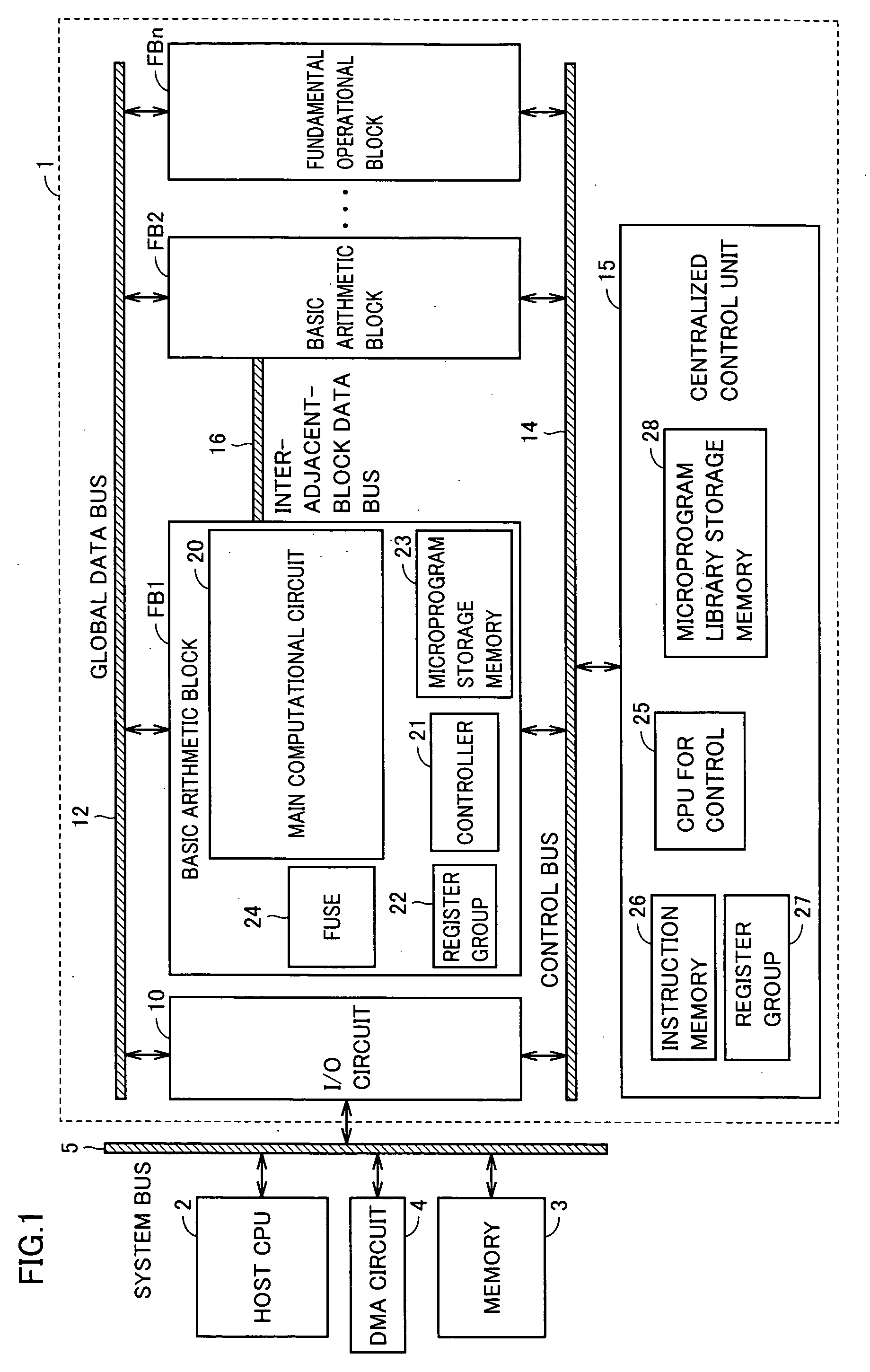
[0125] System LSI 52 has, e.g., a SOC (System On Chip) structure, and includes fundamental operational blocks FB1-FBn coupled in parallel to an internal system bus 54, host CPU 2 controlling processing operat...

second embodiment

[0193]FIG. 18 schematically shows a construction of main computational circuit 20 according to a second embodiment of the invention. Main computational circuit 20 has a memory cell mat 95 in which two-port SRAM cells MCS are arranged in rows and columns. Two-port SRAM cell MCS has substantially the same structure as that shown in FIG. 11.

[0194] In memory cell mat 95, word lines WLV are arranged perpendicular to word lines WLH. Bit line pairs BLHP are arranged parallel and corresponding to word lines WLV, and bit line pairs BLVP are arranged parallel and corresponding to word lines WLH.

[0195] A row decoder 100 selects word line WLH, and a row decoder 102 selects word line WLV. Word line WLV and bit line pair BLHP are connected to SRAM cells MCS included in a common entry ERY.

[0196] The sense amplifier in sense amplifier group 40 and the write driver in write driver group 42 are arranged corresponding to entry ERY, and the arithmetic and logic unit (ALU) in operational processing u...

third embodiment

[0215]FIG. 25 schematically shows a construction of main computational circuit 20 according to a third embodiment of the invention. In main computational circuit 20 shown in FIG. 25, an orthogonal two-port memory cell mat 130 is arranged adjacent to memory cell mat 30. Memory cell mat 30 includes memory cells of a single port construction in rows and columns. Word lines WL are arranged corresponding to memory cell rows, respectively, and shared bit line pairs CBLP0-CBLP(m-1) each shared by memory cell mats 30 and 130 are arranged corresponding to the memory cell columns, respectively.

[0216] In orthogonal two-port memory cell mat 130, bit lines BLVP are arranged perpendicularly to shared bit line pairs CBLP0-CBLP(m-1). Word lines WLV are arranged parallel and corresponding to shared bit line pairs CBLP0-CBLP(m-1), respectively, and word lines WLH are arranged parallel and corresponding to bit line pairs BLVP, respectively. Orthogonal two-port memory cell mat 130 includes two-port me...


PUM


Abstract

An orthogonal memory for transforming arrangements of system bus data and processing data is placed between a system bus interface and a memory cell mat storing the processing data. The orthogonal memory includes two-port memory cells, and changes data train transferred in a bit parallel and word serial fashion into a data train of word parallel and bit serial data. Data transfer efficiency in a signal processing device performing parallel operational processing can be increased without impairing parallelism of the processing.

Description

BACKGROUND OF THE INVENTION [0001] 1. Field of the Invention [0002] The present invention relates to a semiconductor signal processing device, and particularly to a construction of an integrated circuit device for signal processing which can perform fast arithmetic processing of a large quantity of data, using a semiconductor memory. More particularly, the invention relates to a construction for efficiently transferring data to and / or from a semiconductor memory storing arithmetic data. [0003] 2. Description of the Background Art [0004] In accordance with widespread use of portable terminal equipments in recent years, digital signal processing for processing a large quantity of data such as audio and image data at high speed have become more important. Such digital signal processing generally involves a DSP (Digital Signal Processor) as a dedicated semiconductor device. Data processing such as filter processing is performed in digital signal processing of the audio and image data. S...

Claims


Application Information

Patent Timeline
Patent Type & Authority Applications(United States)
IPC IPC(8): G06F15/00G06F7/48
CPCG06F7/785G11C5/025G11C7/1006G11C7/18G11C8/16G11C11/419G11C2207/104
Inventor NODA, HIDEYUKIARIMOTO, KAZUTAMIDOSAKA, KATSUMISAITO, KAZUNORI
Owner RENESAS TECH CORP
Why Eureka
Try Eureka