Gain boosting for tuned differential LC circuits

a differential lc circuit and gain boost technology, applied in the field of communication systems, can solve the problems of many technical hurdles that need to be overcome before monolithic integration of transceivers, increase component mismatches in the cmos process, and difficulty in designing the device for wireless communication devices

Inactive Publication Date: 2006-07-06
AVAGO TECH WIRELESS IP SINGAPORE PTE
View PDF6 Cites 51 Cited by
  • Summary
  • Abstract
  • Description
  • Claims
  • Application Information

AI Technical Summary

Benefits of technology

[0011] In accordance with various embodiments of the present invention, a method and apparatus provide for gain level boosting in a low noise amplifier (such as a differential low noise amplifier circuit at the front end of a receiver circuit formed on an integrated circuit) by selectively coupling an adjustable negative transconductance circuit between an amplifier circuit and an output tank circuit to effectively generate an adjustable negative transconductance value to compensate for any losses generated by the output tank circuit. For example, when the adjustable negative transconductance circuit is implemented with a pair of cross-coupled NMOS transistors, the adjustable negative transconductance value may be added or removed from the low noise amplifier by turning the negative transconductance circuit off in response to a power down signal and turning the negative transconductance circuit on in response to a power up signal. In addition or in the alternative, the adjustable negative transconductance value may be adjusted by increasing the amount of current supplied to the adjustable negative transconductance circuit in response to temperature changes, and / or by using a digitally controlled current source to provide different current levels to the adjustable negative transconductance circuit.

Problems solved by technology

As the demand for enhanced performance (e.g., reduced interference and / or noise, improved quality of service, compliance with multiple standards, increased broadband applications, et cetera), smaller sizes, lower power consumption, and reduced costs increases, wireless communication device engineers are faced with a very difficult design challenge to develop such a wireless communication device.
Even though CMOS technology has provided a lot of attractions, there are still many technical hurdles needed to be overcome before monolithic integration of a transceiver is possible.
For example, the CMOS process increases component mismatches, increases temperature related variations, and increases process variations.
One challenge that is encountered in the design and manufacture of RF signal integrated circuits relates to the design of a low noise amplifier (LNA) that provides adequate signal amplification without degrading the signal to noise ratio (SNR) significantly.
When such amplifiers use output resonant tank circuits to increase the gain of the amplifier at the desired operating frequency, resistive losses resulting from non-idealities in such output tank circuits can limit or degrade the amount of gain generated by the amplifier by imposing an upper limit on the input impedance of the tank circuit.

Method used


Image

  • Gain boosting for tuned differential LC circuits
  • Gain boosting for tuned differential LC circuits
  • Gain boosting for tuned differential LC circuits

Examples


Embodiment Construction

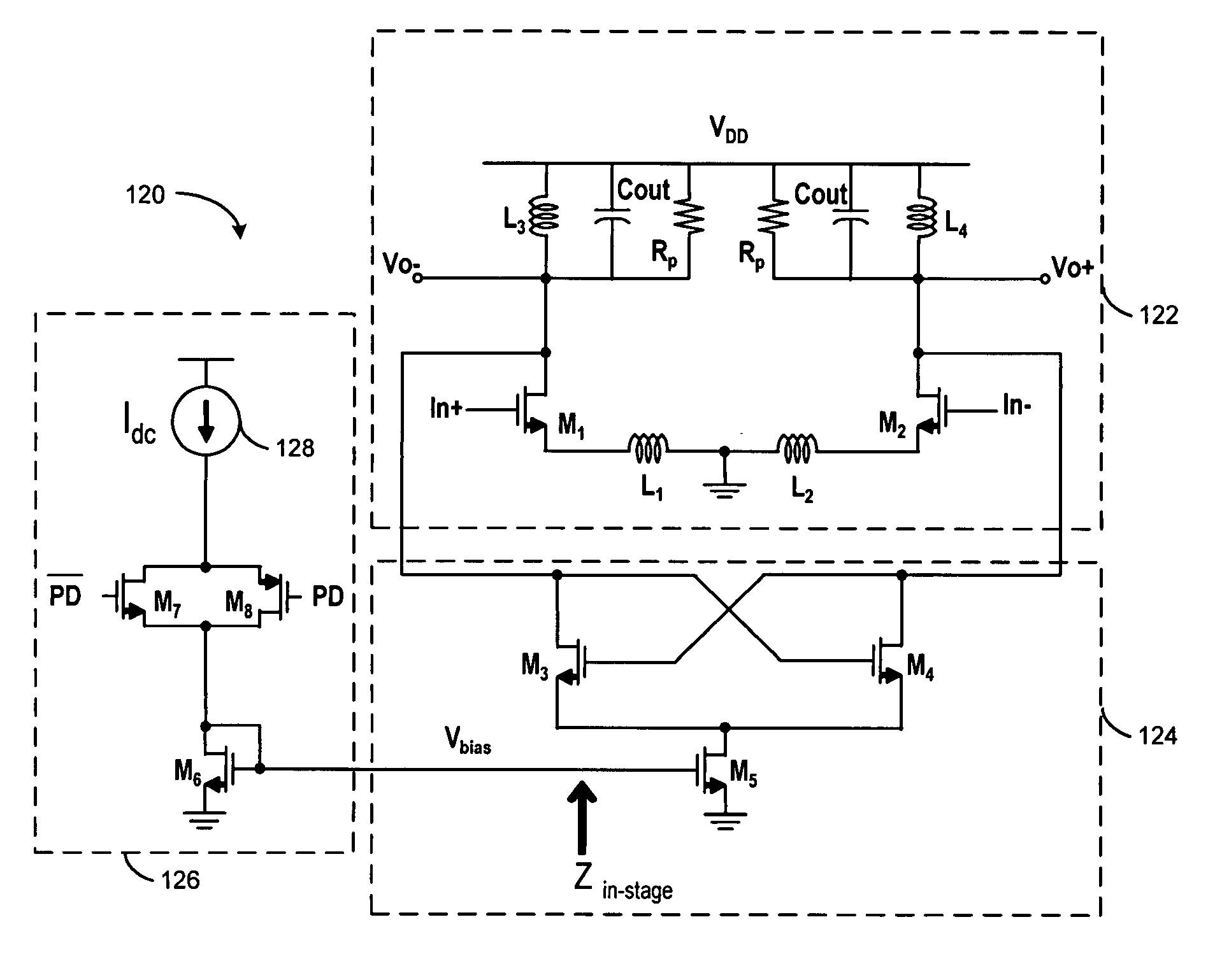
[0022] A method and apparatus are described for boosting the gain of an amplifier circuit by selectively controlling a negative resistance stage connected to a low noise amplifier output tank. While various details are set forth in the following description, it will be appreciated that the present invention may be practiced without these specific details. For example, selected aspects are shown in block diagram form, rather than in detail, in order to avoid obscuring the present invention. Some portions of the detailed descriptions provided herein are presented in terms of schematic descriptions and circuit depictions which are used by those skilled in the field of communication systems to describe and convey the substance of their work to others skilled in the art.

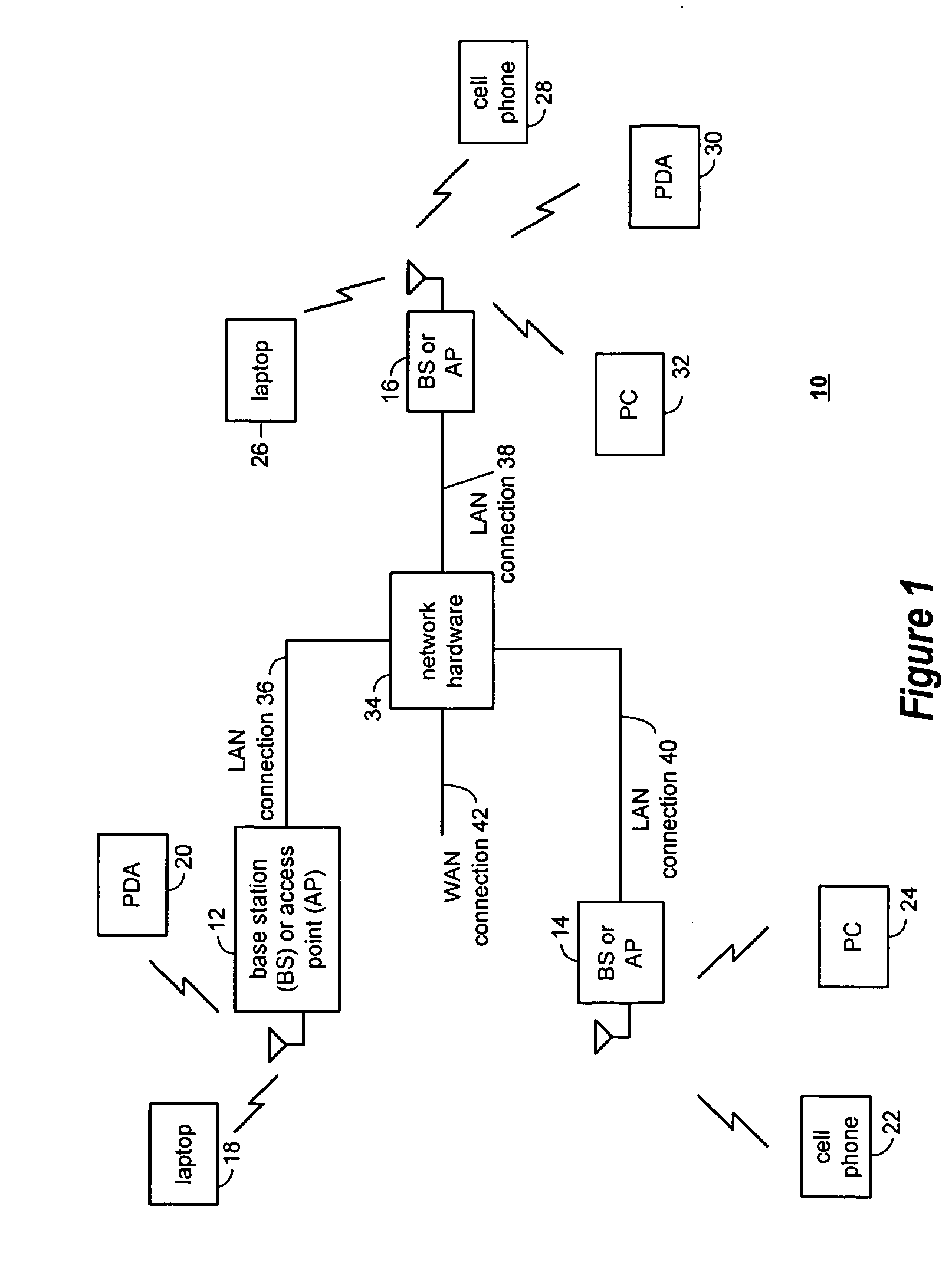
[0023]FIG. 1 illustrates a wireless communication system 10 in which embodiments of the present invention may operate. As illustrated, the wireless communication system 10 includes a plurality of base stations and / or acc...


PUM


Abstract

A gain boost circuit and methodology are described for providing improved gain boosting with tuned amplifier circuits, such as differential low noise amplifier circuits having output resonant tank circuits. By selectively controlling the current source for a negative transconductance stage coupled between the differential amplifier output and the output resonant tank circuits, the amplifier gain may be adjusted to compensate for temperature variations. In addition, the amplifier gain boost may be selectively added, removed or even incrementally adjusted by using a current source control circuit in the negative transconductance stage to adjust the negative transconductance value generated by the negative transconductance stage.

Description

BACKGROUND OF THE INVENTION [0001] 1. Field of the Invention [0002] The present invention is directed in general to communication systems. In one aspect, the present invention relates to a method and system for improving the gain boost of a low noise amplifier. [0003] 2. Related Art [0004] Communication systems are known to support wireless and wire lined communications between wireless and / or wire lined communication devices. Such communication systems range from national and / or international cellular telephone systems to the Internet to point-to-point in-home wireless networks. Each type of communication system is constructed, and hence operates, in accordance with one or more communication standards. For instance, wireless communication systems may operate in accordance with one or more standards including, but not limited to, IEEE 802.11, Bluetooth, advanced mobile phone services (AMPS), digital AMPS, global system for mobile communications (GSM), code division multiple access (...

Claims


Application Information

Patent Timeline
Patent Type & Authority Applications(United States)
IPC IPC(8): H03F3/45
CPCH03F3/195H03F3/45183H03F2200/294H03F2200/372H03F2203/45288H03F2203/45318H03F2203/45464H03F2203/45544H03F2203/45638H03F2203/45704H03G1/04H03G3/001
Inventor LEETE, JOHN
Owner AVAGO TECH WIRELESS IP SINGAPORE PTE
Why Eureka
Try Eureka