Method to fabricate a thin film non volatile memory device scalable to small sizes

a memory device and non-volatile technology, applied in semiconductor devices, digital storage, instruments, etc., can solve the problems of insufficiently addressing these needs, brittleness, and high cost of 5 per tag, and achieve the effect of small memory arrays that are economically feasible, thin, inexpensive and robus

Inactive Publication Date: 2006-07-13
TERECIRCUITS CORP
View PDF8 Cites 10 Cited by
  • Summary
  • Abstract
  • Description
  • Claims
  • Application Information

AI Technical Summary

Benefits of technology

[0010] The thin film non-volatile memory is an optoelectronic cross bar memory comprising a photoconductive thin film sandwiched between two electrodes, together with a radiation source to provide irradiation to the photoconductive thin film. Under an electric field and visible irradiation, non-volatile charges are generated and stored in the photoconductive thin film and then can be read with appropriate charge sensing circuit. This effect is highly stable and repeatable, and is the basis for the present invention thin film non-volatile memory.
[0011] The control circuitry of the present invention is based on thin film silicon technology, in which thin film transistors are fabricated on plastic substrates, preferably in a process amenable to roll-to-roll processing. This potentially reduces cost and makes it possible to conveniently transfer the ICs to end-product substrates at an arbitrary density and position.
[0013] The present invention improves substantially to make small memory arrays economically, which is desirable for the smart tag / smart card applications, with the attendant requirement of thin, inexpensive and robust devices that can be incorporated into paper-thin products. The invention scales well to larger sizes as well.

Problems solved by technology

Current products do not adequately address these needs.
Conventional silicon chips are thick (0.5 mm before thinning), brittle, and too expensive to meet the <5¢ per tag cost target that most customers quote.
Even after this, the product has problems, including the fragility of the chip-antenna connection and remaining thickness of silicon.
It will be very difficult to incorporate such devices unobtrusively into paper documents.
Another major difficulty with existing solutions is that conventional silicon nonvolatile memory (which comes in two closely related varieties: EEPROM, or electrically erasable and programmable read-only memory, and FLASH memory) is substantially more expensive than CMOS logic circuitry, and requires a different IC process, so that it is often not fabricated in the same chip or at the same time or using the same fabrication processes as logic.
Such connections substantially increase the cost of the product, as well as lowering reliability.
Such nonvolatile memory chips are not only more expensive per unit area than logic chips or volative memory such as DRAM and SRAM, but they cannot be easily scaled to small sizes such as are desired for RFID tags (as well as other products, such as smart cards).
Thus, one is again confronted with the difficulty of getting the amount of circuitry needed at an acceptable price.

Method used


Image

  • Method to fabricate a thin film non volatile memory device scalable to small sizes
  • Method to fabricate a thin film non volatile memory device scalable to small sizes
  • Method to fabricate a thin film non volatile memory device scalable to small sizes

Examples


Embodiment Construction

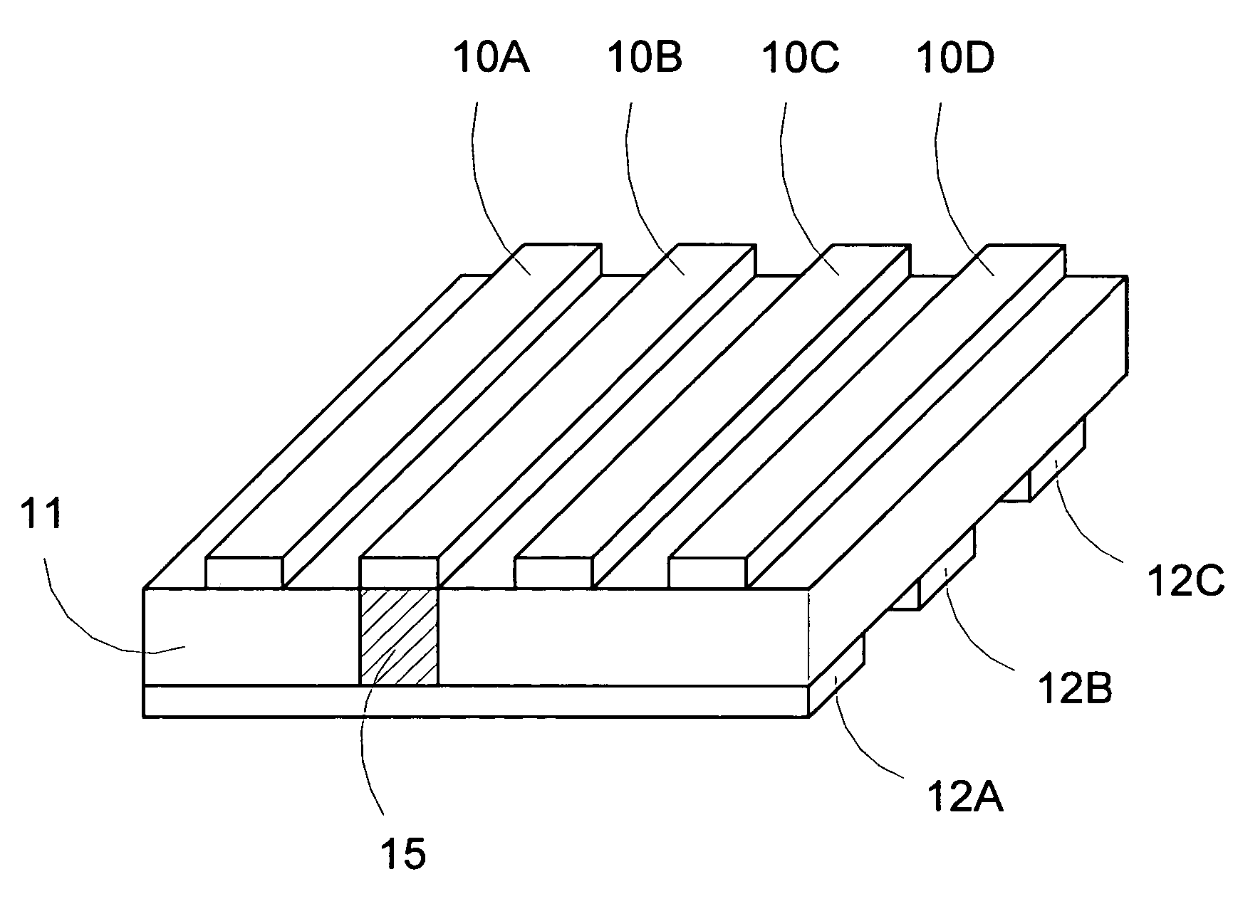
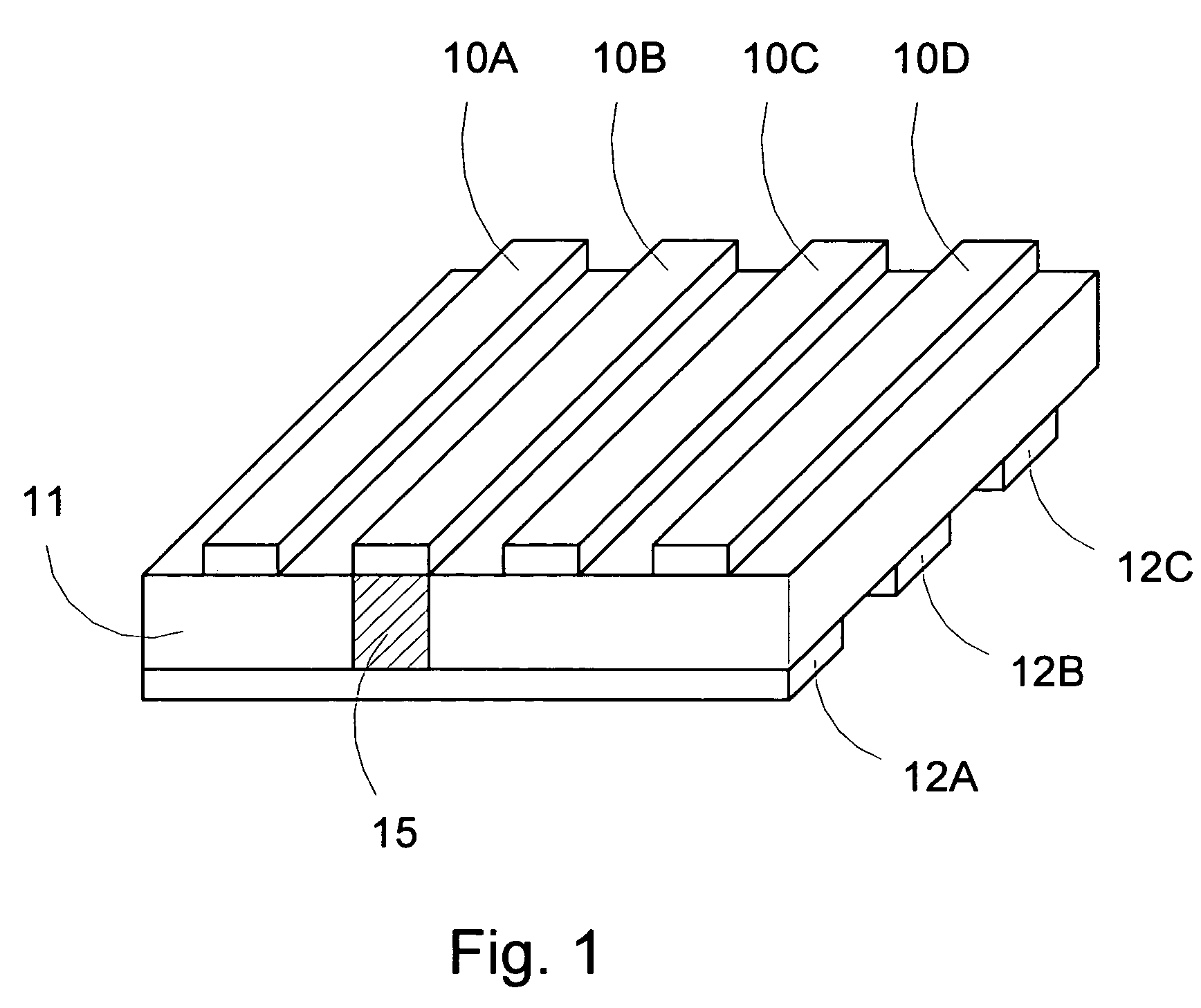
[0018] Thin film silicon technology, in which thin film transistors are fabricated on plastic substrates, is reasonably well known and well documented. The thin film transistors (TFTs) resulting from these processes, which use amorphous silicon (a-Si) as the active semiconductor material, are suitable for general computational operations as well as other applications such as display switching elements. They can be used to read and write information from EEPROM cells, for example, as well as to make oscillators and logic gates. Because they are fabricated on plastic substrates, the process is amenable to adaptation to roll-to-roll processing with attendant cost reductions, and the substrate can be sufficiently thin that it is easily accommodated in the thin RFID devices and smart tags or cards which are the primary (though not exclusive) focus of this invention.

[0019] The prior art memory cells, while satisfactory to store digital information, do not meet the needs of the applicatio...


PUM


Abstract

A thin film non volatile memory scalable to small sizes and its fabrication process are disclosed. The thin film memory comprises a thin film transistor control circuitry fabricated on a flexible substrate, together with an optoelectronic cross bar memory comprising a photoconducting material. The thin film non volatile memory can be used in RFID communication tag with the control circuitry further comprises wireless communication circuitry such as an antenna, a receiver, and a transmitter.

Description

FIELD OF THE INVENTION [0001] This invention is related to the provision of small, thin information appliances or computing devices which have a need for nonvolatile rewriteable digital memory. BACKGROUND OF THE INVENTION [0002] Currently there is a strong trend toward the development of very low cost RFID tags, relatively small scale integrated circuits whose input and output, via radio frequency radiation, uses transponders rather than receivers and transmitters, which are cheap enough to achieve ubiquitous deployment on essentially any object whose location and movement are of interest. Such tags would simplify and expedite many tasks, including keeping track of and streamlining inventories, preventing theft and counterfeiting, guaranteeing product authenticity, and monitoring environmental conditions experienced by the object. Preferably they should be available in the form of labels which can be easily attached to objects. Some objects, such as secure papers (for example curren...

Claims


Application Information

Patent Timeline
Patent Type & Authority Applications(United States)
IPC IPC(8): G11C13/04
CPCH01L31/161H01L51/0034H01L51/0077H01L51/0078H01L51/4206H10K85/10H10K85/311H10K85/30H10K30/451
Inventor SHEATS, JAMES
Owner TERECIRCUITS CORP
Why Eureka
Try Eureka