Capacitor material with metal component for use in circuitized substrates, circuitized substrate utilizing same, method of making said circuitized substrate, and information handling system utilizing said circuitized substrate
a technology of circuitized substrates and capacitors, which is applied in the direction of fixed capacitors, connection contact materials, printed capacitor incorporation, etc., can solve the problems of inability of the dielectric layer to withstand substantial voltage, obstacles to the formation of thru-holes, and further undesirable effects
- Summary
- Abstract
- Description
- Claims
- Application Information
AI Technical Summary
Benefits of technology
Problems solved by technology
Method used
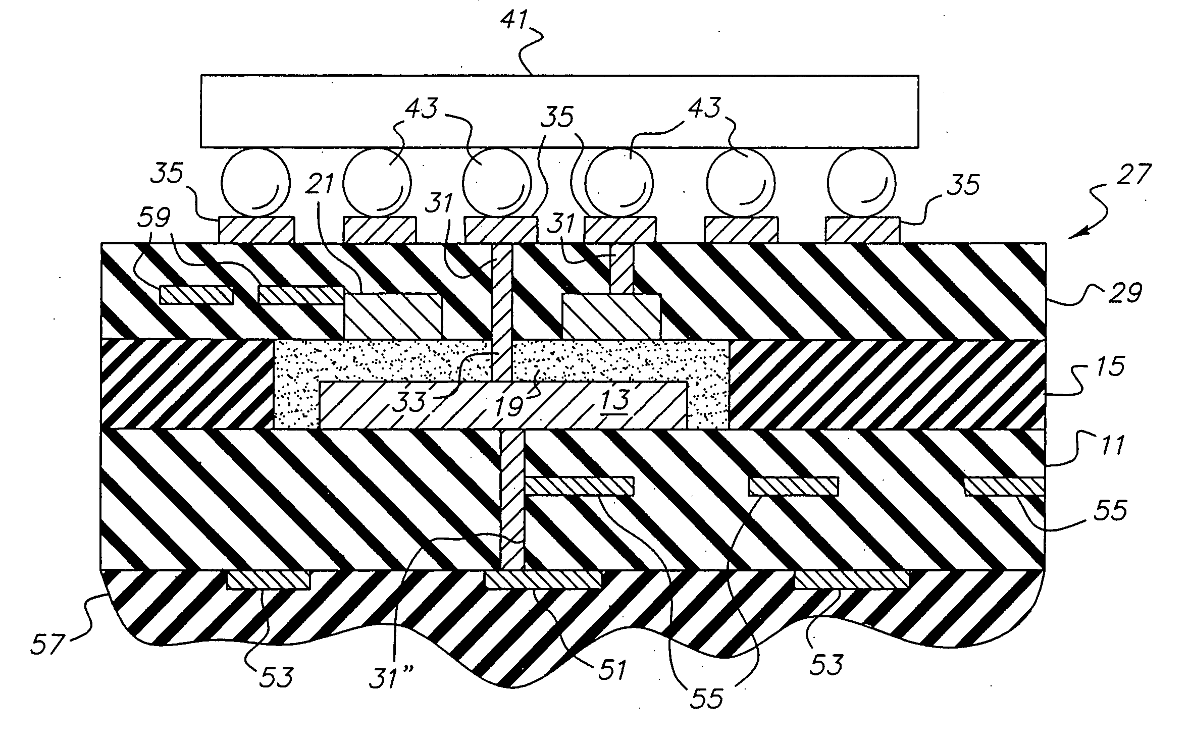
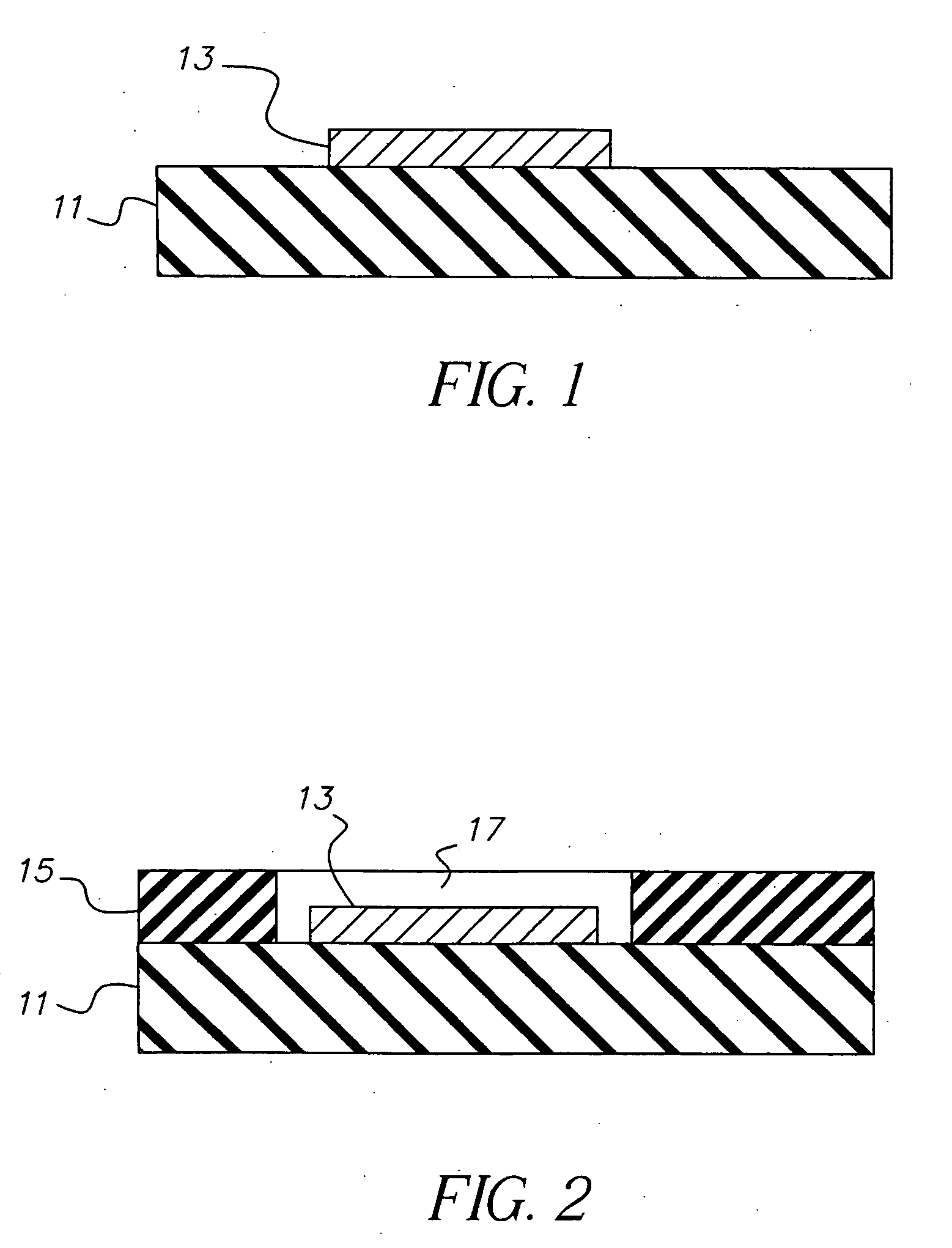
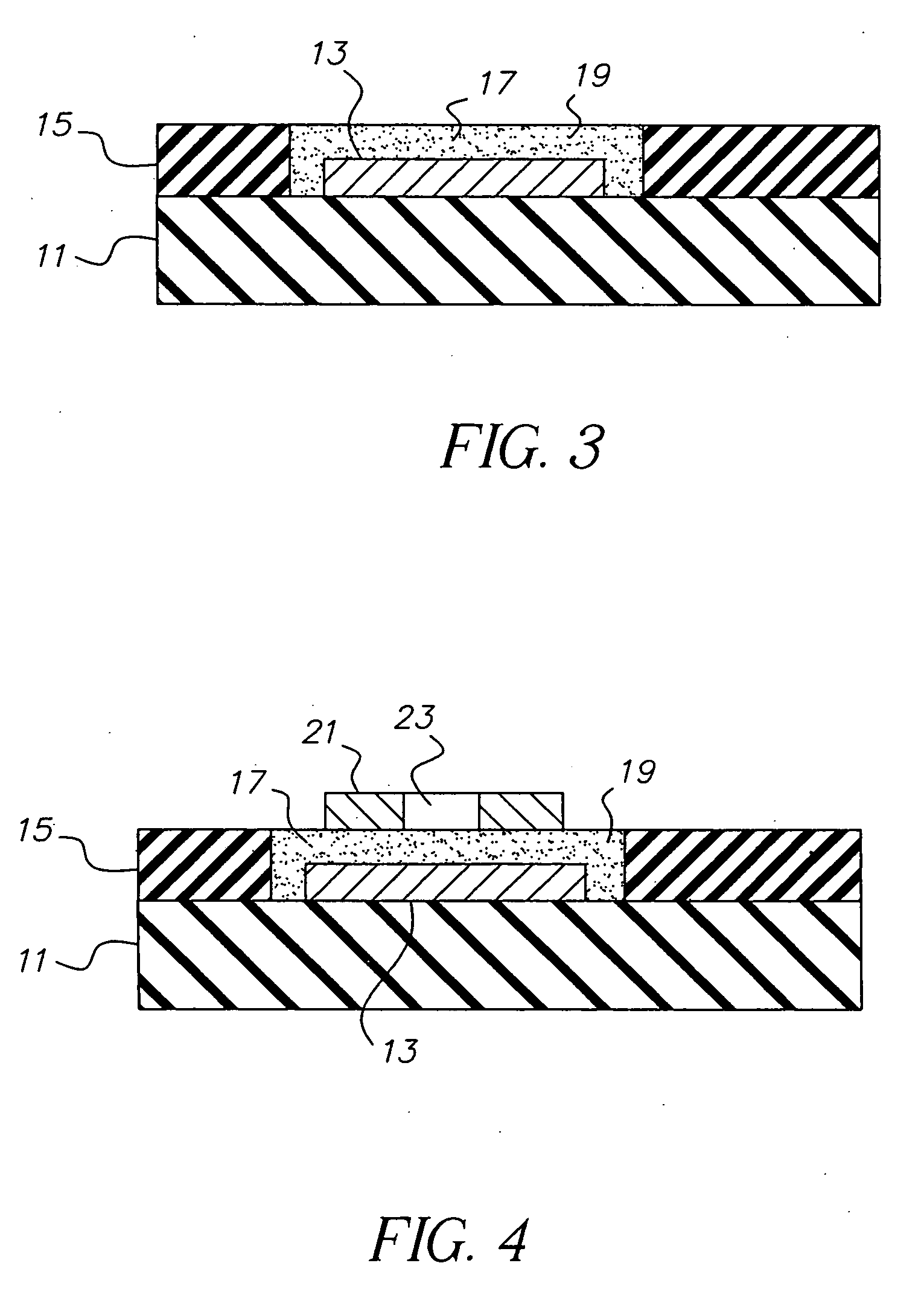
Image

Examples
example one
[0063] 38.5 grams (gm) of an epoxy novolac resin sold under the product name “LZ 8213” from Huntsman, Salt Lake City, Utah, containing about 35 wt % methyl ethyl ketone and 6.5 gm of a phenoxy resin sold under the product name “PKHC” from Phenoxy Associates, Rock Hill, S.C., containing 50 wt % methyl ethyl ketone were mixed together with 100 gm of barium titanate (BaTiO3) powder available from Cabot Corporation, Boyertown, Pa. ((50 gm BaTiO3 with mean particle size=0.065 micron, surface area=16 m2 / gm) and (50 gm BaTiO3 with mean particle size=0.12 micron, surface area=8.2 m2 / gm)), 13 gm propylene glycol methyl ether acetate) and 12 gm methyl ethyl ketone) and ball milled for 3 days. After 3 days of ball milling, an homogeneous slurry was observed. 50 gm of this mixed slurry was mixed with 20 gm silver nano-powders available from Cima NanoTech, Inc., North Industrial Park, Caesarea, Israel, having a D90 particle size of 0.07 micron (D90 meaning 90% of the particles have a diameter le...
example two
[0064] 30.7 gm of “LZ 8213” epoxy novolac resin containing about 35 wt % methyl ethyl ketone and 5.3 gm of “PKHC” phenoxy resin containing 50 wt % methyl ethyl ketone were mixed together with 100 gm of Cabot barium titanate having a mean particle size of 0.12 micron and particle surface area of about 8.2 m2 / gm, 12 gm propylene glycol methyl ether acetate and 15 gm methyl ethyl ketone, and ball milled for 3 days until a homogeneous slurry was observed. 51.6 gm of this mixed slurry was then mixed with 5.1 gm of Cima NanoTech's silver nano-powders having a D90 particle size of 0.07 micron and 10 gm methyl ethyl ketone and ball milled for 5 days. A thin film of this mixed composite was then deposited on a copper substrate and dried at approximately 140° C. for 3 minutes in an oven to remove residual organic solvents. This was followed by curing in an oven at 190° C. for 2 hours. A second electrical conductor was then formed using a sputtering operation atop the cured film using a mask n...
example three
[0065] 30.7 gm of “LZ 8213” epoxy novolac resin containing about 35 wt % methyl ethyl ketone and 5.3 gm of“PKHC” phenoxy resin containing 50 wt % methyl ethyl ketone were mixed together with 100 gm of Cabot barium titanate having a mean particle size of 0.12 micron and particle surface area of about 8.2 m2 / gm, 12 gm propylene glycol methyl ether acetate and 15 gm methyl ethyl ketone, and ball milled for 3 days until a homogeneous slurry was observed. 30.5 gm of this mixed slurry was mixed with 10.4 gm of Cima NanoTech's silver nano-powders having a D90 particle size of 0.07 micron and 10 gm methyl ethyl ketone and ball milled for 5 days. A thin film of this mixed composite was then deposited on a copper substrate and dried at approximately 140° C. for 3 minutes in an oven to remove residual organic solvents. This was followed by curing in an oven at 190° C. for 2 hours. A second electrical conductor was then formed using a sputtering operation atop the cured film using a mask normal...
PUM
| Property | Measurement | Unit |
|---|---|---|
| surface area | aaaaa | aaaaa |
| particle size | aaaaa | aaaaa |
| glass transition temperature | aaaaa | aaaaa |
Abstract
Description
Claims
Application Information
 - R&D
- Intellectual Property
- Life Sciences
- Materials
- Tech Scout
- Unparalleled Data Quality
- Higher Quality Content
- 60% Fewer Hallucinations
Browse by: Latest US Patents, China's latest patents, Technical Efficacy Thesaurus, Application Domain, Technology Topic, Popular Technical Reports.
© 2025 PatSnap. All rights reserved.Legal|Privacy policy|Modern Slavery Act Transparency Statement|Sitemap|About US| Contact US: help@patsnap.com