Circuit board, electronic device employing circuit board, and mehtod of producing circuit board

a technology of electronic devices and circuit boards, applied in the field of circuit boards, can solve the problems of reduced battery life, increased power consumption, and increased size of buffer circuits, and achieve the effects of reducing crosstalk, reducing power consumption, and reducing power consumption

Inactive Publication Date: 2006-07-20
OHMI +1
View PDF5 Cites 28 Cited by
  • Summary
  • Abstract
  • Description
  • Claims
  • Application Information

AI Technical Summary

Benefits of technology

[0056] In the present invention, since a circuit board using a magneto-dielectric can be formed in multilayers, various electronic devices can be configured to achieve low power consumption. By using the magneto-dielec...

Problems solved by technology

There has been a problem that since such a signal transmission line formed on the circuit board such as the printed wiring board generally has a low characteristic impedance of 50Ω, it is necessary to flow a large current for propagating a signal in the transmission line so that a buffer circuit increases in size and the power consumption increases.
Particularly in portable devices such as portable telephones, there has arisen a serious problem that flowing a large current causes a reduction in battery life, and so forth.
However, there has been a problem that the characteristic impedance of a normal transmission line has an upper limit of about 200 to 300Ω and therefore a sufficient power consumpt...

Method used


Image

  • Circuit board, electronic device employing circuit board, and mehtod of producing circuit board
  • Circuit board, electronic device employing circuit board, and mehtod of producing circuit board
  • Circuit board, electronic device employing circuit board, and mehtod of producing circuit board

Examples


specific example

[0131] Hereinbelow, the present invention will be described based on further detailed specific examples, but the present invention is not limited to these specific examples.

specific example 1

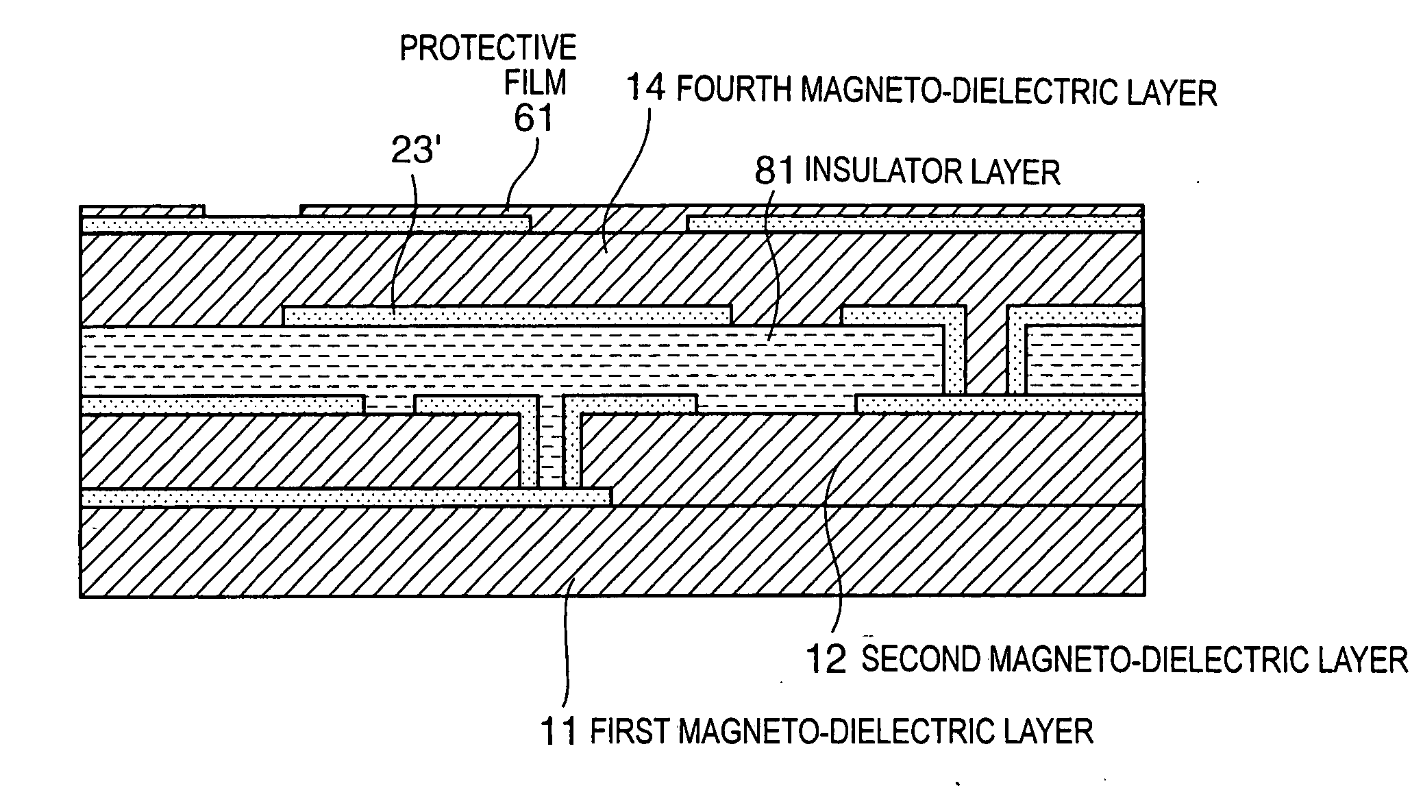
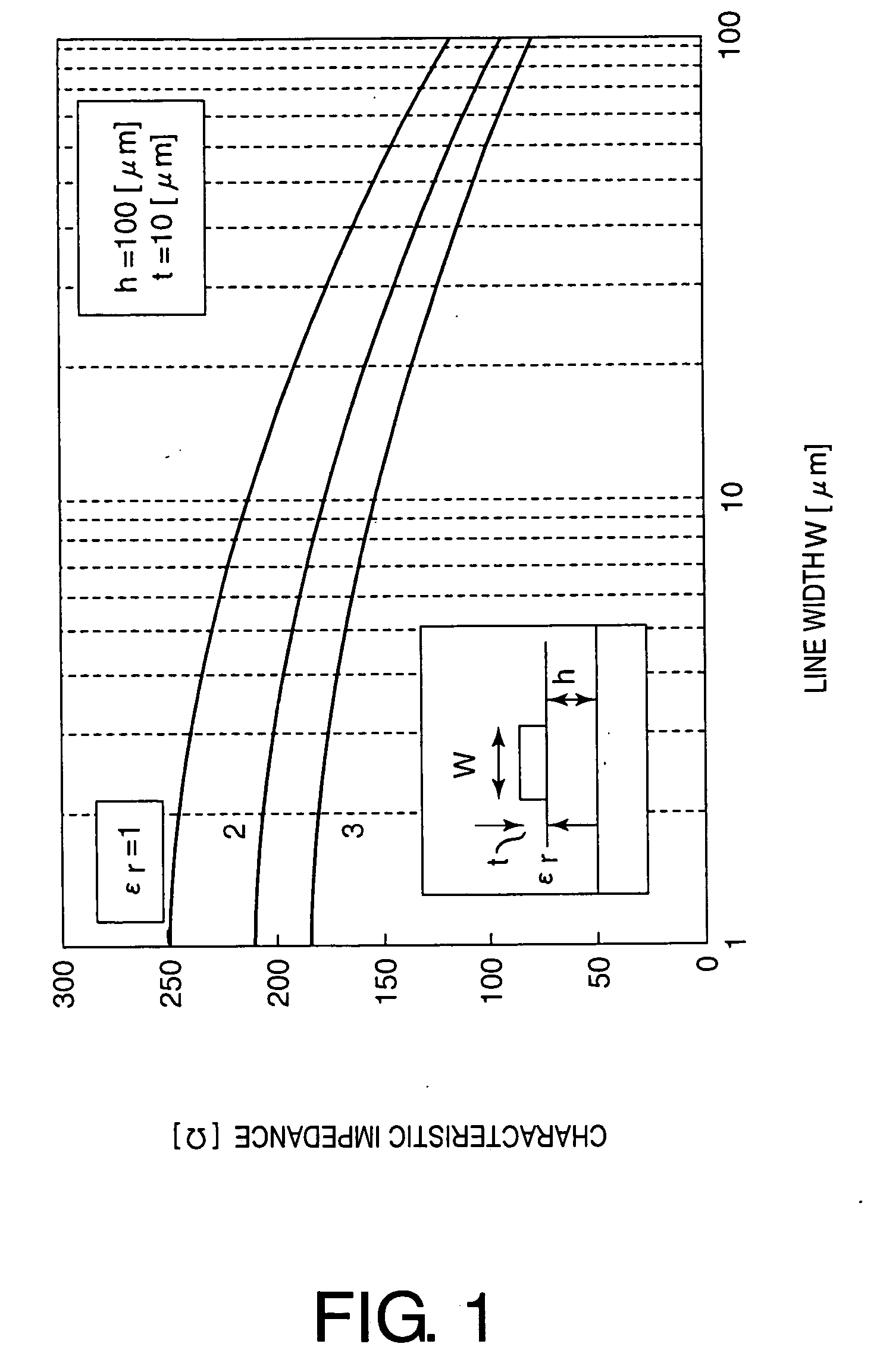
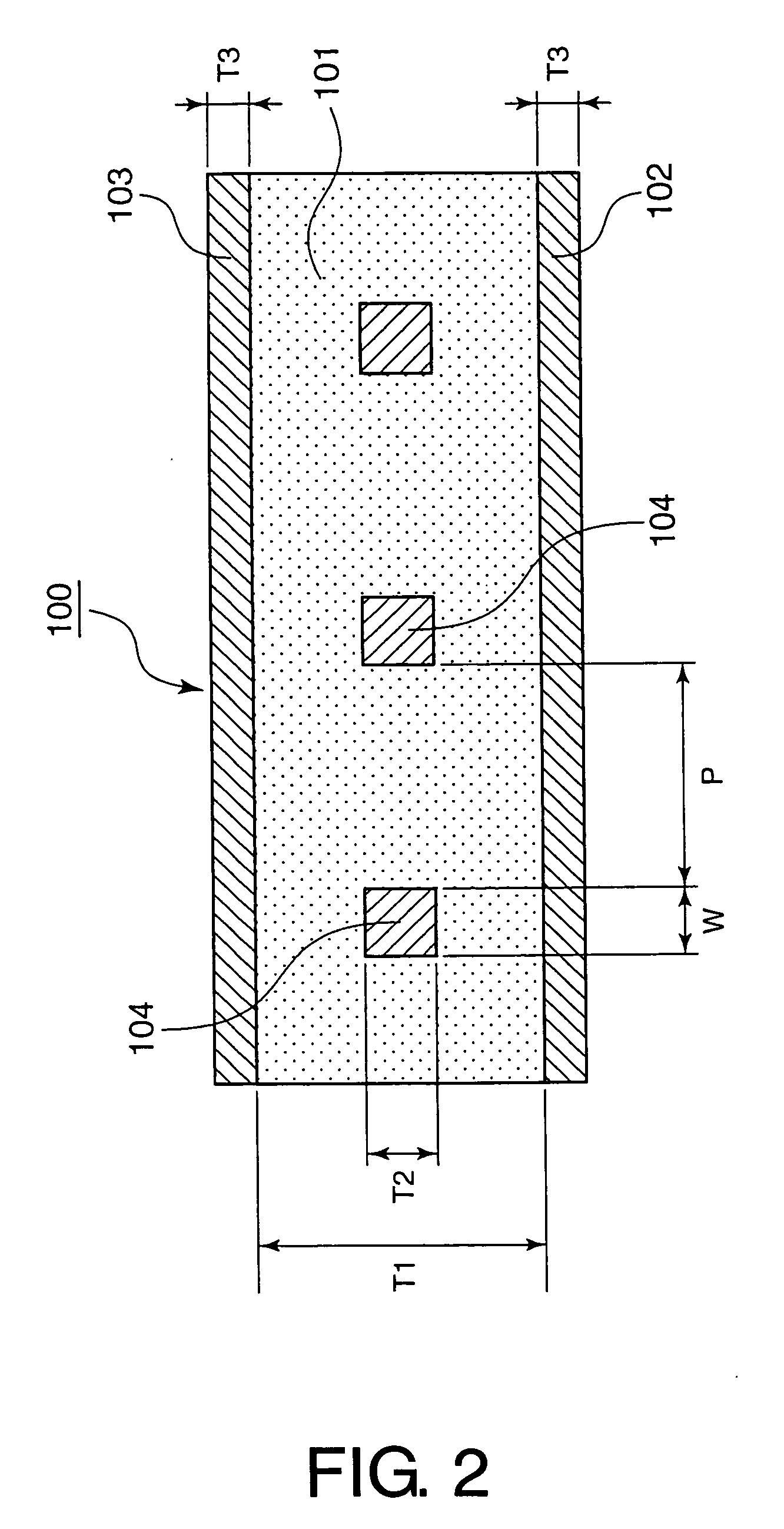
[0132] A ferrite material (produced by Toda Kogyo Corporation) in the form of fine magnetic powder formed by insulators was uniformly dispersed into a wax obtained by dissolving, into a solvent, 100 parts of a polycycloolefin resin (denatured ring-opened polymer of norbornene-type cycloolefin (Tg=170° C.)), 40 parts of a bisphenol-based curing agent, and 0.1 parts of an imidazole-based effect accelerator, then, after casting, a heat treatment was applied thereto, thereby obtaining a first insulator 101 having a thickness T1=100 μm shown in FIG. 2. A relative permittivity ε of this first insulator 101 was 2.9. The ratio of a dispersion amount of the magnetic powder was 100 weight parts relative to 100 weight parts of the components of the wax other than the solvent.

[0133] Note that lines 104 formed by a copper metal and each having a sectional width W of 10 μm and a sectional thickness T2 of 10 μm were buried inside the first insulator 101 so as to be arranged at a wiring interval P...

specific example 2

[0139] A wiring board was produced in the same manner as Specific Example 1 except that the dispersion amount of the magnetic powder in the first insulator 101 was changed and the permeability of the first insulator 101 at 100 MHz was changed in the range of 1 to 100. A relationship between the characteristic impedance of a transmission line formed in the wiring board 100 and the relative permeability of the first insulator 101 is shown in FIG. 15. It has been confirmed that it is possible to obtain a transmission line having a characteristic impedance of 500Ω with a relative permeability of about 25 and a characteristic impedance of 1000Ω with a relative permeability of about 100.


PUM


Abstract

A circuit board (100) having an insulator layer and a conductor (104) buried in the insulator layer, wherein the insulator layer has a first insulator (101) satisfying a relation μr≧εr, assuming εr is the dielectric constant and μr is the relative permeability, and the conductor is substantially surrounded by the first insulator.

Description

TECHNICAL FIELD [0001] The present invention relates to a circuit board used as, for example, a high-frequency printed wiring board or the like and, more specifically, relates to a circuit board that consumes low current, has an excellent function of suppressing crosstalk and radiation noise, and can improve the quality of a signal propagating in a line. The present invention also relates to an electronic device employing the circuit board and a method of producing the circuit board. BACKGROUND ART [0002] Microstrip lines, striplines, and so forth widely used as high-frequency signal transmission lines are formed on circuit boards such as printed wiring boards and used in various electronic devices such as portable telephones, personal computers, and household electric devices. [0003] It is general that use is normally made of 50Ω as a characteristic impedance of the foregoing signal transmission line. [0004] Further, in order to supply a sufficient signal to this 50Ω line from an a...

Claims


Application Information

Patent Timeline
IPC IPC(8): H05K1/03H05K1/18H05K1/00H05K1/02
CPCH05K1/024H05K3/4676H05K3/4688H05K1/02H05K1/03
Inventor OHMI, TADAHIROSUGAWA, SHIGETOSHIMORIMOTO, AKIHIROKATO, TAKEYOSHI
Owner OHMI
Why Eureka
Try Eureka