Sputtering target, dielectric film formed from the sputtering target and method for producing the dielectric film

Inactive Publication Date: 2006-07-20
NIPPON SHEET GLASS CO LTD
View PDF0 Cites 14 Cited by
  • Summary
  • Abstract
  • Description
  • Claims
  • Application Information

AI Technical Summary

Benefits of technology

[0025] The invention further provides a method of producing a dielectric film, including the step of forming a thin film by a sputtering technique with use of a sputtering target defined above, wherein the concentration of oxygen contained in a sputtering gas is not higher than 2%. By this condition, stable film formation can be made, so that a high refractive index optical thin film few in defects and

Problems solved by technology

The former film forming technique has a problem that the film forming speed is low, and has a problem that discharge becomes unstable because the surface of the target is covered with an electrically insulating oxide in a sputtering process to thereby cause arcing.
This method is limited in the case where the size of the target is small.
As the size of the target increases, uniform discharge cannot be kept because of the relation between the wavelength of the high-frequency voltage and the size of the target to thereby make it substantially difficult to form a film.
When a DC bias is applied to a TiOx target in an argon gas atmosphere to form a film having a high refractive index, there is however a problem that a film defect is formed because dust generated by fine destruction of a surface of the target is deposited on the surface of the substrate.
It is however impossible to use the thin film industriallybecausethethinfilmhasalotof drawbacks.
It is difficult to use the thin f

Method used


Image

  • Sputtering target, dielectric film formed from the sputtering target and method for producing the dielectric film
  • Sputtering target, dielectric film formed from the sputtering target and method for producing the dielectric film
  • Sputtering target, dielectric film formed from the sputtering target and method for producing the dielectric film

Examples


Embodiment Construction

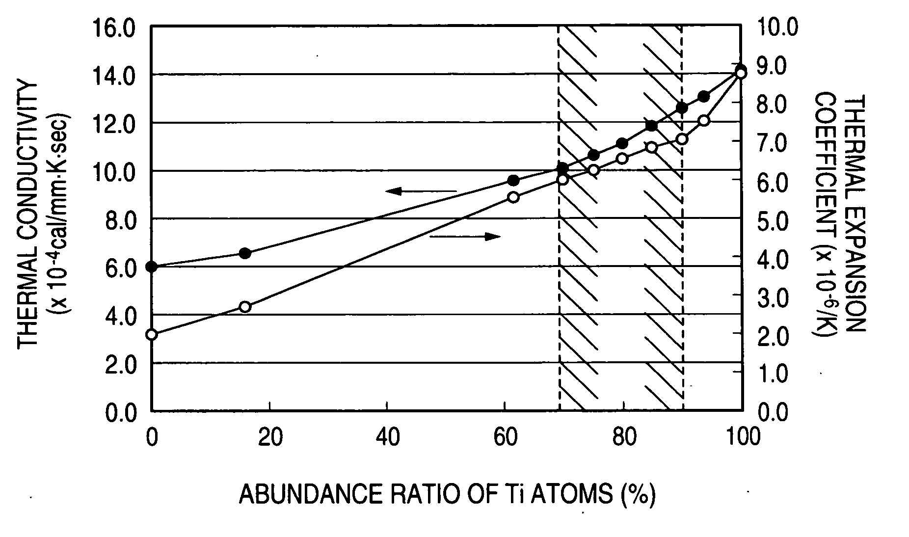
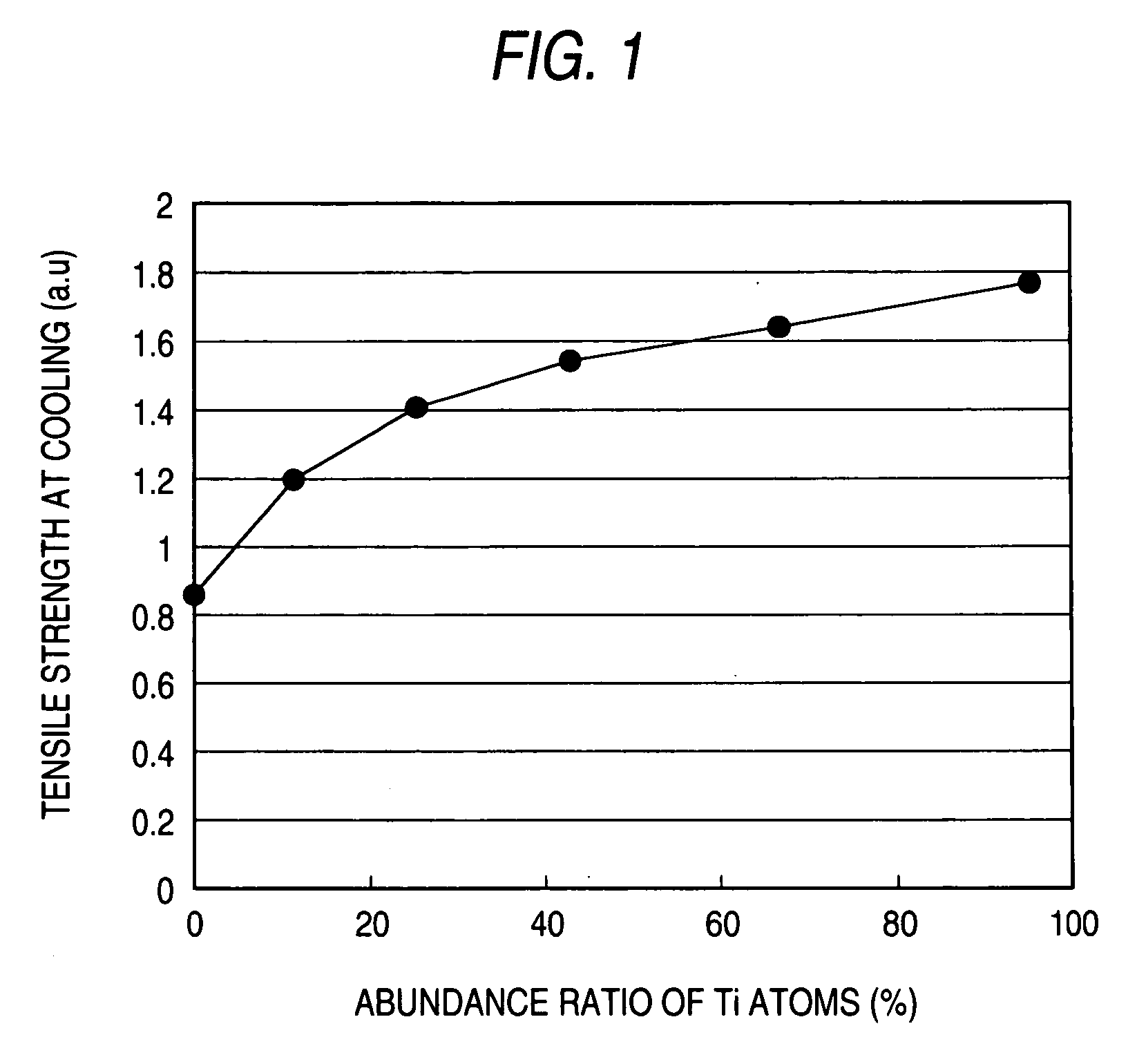
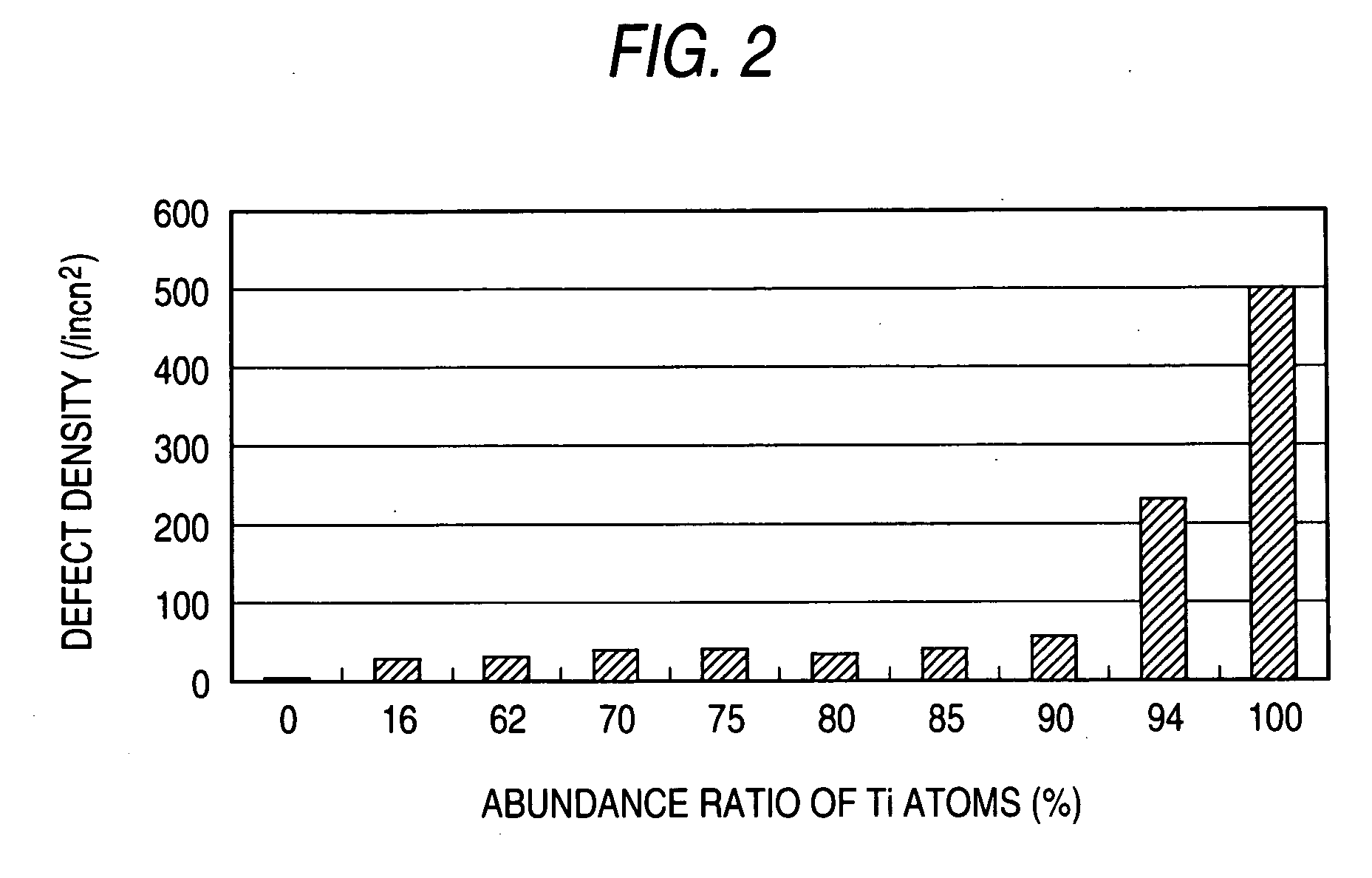
[0030] The invention is based on the inventors' finding that fine destruction of a surface of a target mainly containing TiOx is caused by thermal stress during sputtering film formation. Although thermal stress generated in the target surface varies in accordance with physical properties of the target material such as thermal conductivity, thermal expansion coefficient, Yong's modulus, specific heat, etc., it mainly depends on the two physical properties of thermal expansion coefficient and thermal conductivity.

[0031] Therefore, sintered bodies were produced while the mixture ratio of TiOx to NbOx in the material was changed. TiOx mentioned here is an oxide of excessive Ti represented by 12 compared with TiO2. Similarly, NbOx is an oxide of excessive Nb represented by 22O5. The thermal conductivity and thermal expansion coefficient of the produced sintered body were measured by a laser flash method and with a thermomechanical analyzer, respectively.

[0032] The value of stress gene...


PUM

PropertyMeasurementUnit
Fractionaaaaaaaaaa
Fractionaaaaaaaaaa
Fractionaaaaaaaaaa

Abstract

A sputtering target according to the invention including an oxide sintered body containing NbOx and TiOx in which the abundance ratio of Ti atoms in the target is from 70% to 90% both inclusively. Preferably, the oxide sintered body has a specific resistance value not higher than 10Ω·cm. Preferably, theoxidesinteredbody has a thermal expansion coefficient not larger than 7 ×10⁻⁶/K and a thermal conductivity not lower than 10 ×10−4 cal/mm-K-sec.

Description

BACKGROUND OF THE INVENTION [0001] 1. Field of the Invention [0002] The present invention relates to a sputtering target used in a sputtering technique for forming a dielectric film chiefly used in the field of optical technology. Particularly it relates to a composite oxide target material for forming a dielectric optical thin film having a high refractive index. [0003] 2. Related Art [0004] Optical thin films are used widely in display devices such as liquid crystal display elements, optical parts for optical communication, optical disks and various. kinds of products such as building window glass, automobile windshield, etc. [0005] In an optical multilayer film which is a laminate of these optical thin films, thin films with a high refractive index are used in combination with thin films with a low refractive index so that an optical interference effect can be used. From this fact, a transparent material having a high refractive index is very important. [0006] An oxide dielectric...

Claims


Application Information

Patent Timeline
IPC IPC(8): B32B9/00
CPCC04B35/46C04B35/495C04B2235/3237C04B2235/3251C04B2235/3253C04B2235/96C04B2235/9607C23C14/083C23C14/3414A47J36/24A47J36/32
Inventor KUNISADA, TERUFUSAOGINO, ETSUOIKADAI, MASAHIRO
Owner NIPPON SHEET GLASS CO LTD
Why Eureka
Try Eureka