Integrated microfludic control employing programmable tactile actuators

a microfluidic control and tactile actuator technology, applied in the direction of positive displacement liquid engines, instruments, laboratory glassware, etc., can solve the problems of inability to individually address control sites, limited number of individually actuated components, and enormous difficulties in device fabrication, etc., to achieve the effect of low cost and easy operation

Inactive Publication Date: 2006-07-27
RGT UNIV OF MICHIGAN
View PDF16 Cites 58 Cited by
  • Summary
  • Abstract
  • Description
  • Claims
  • Application Information

AI Technical Summary

Benefits of technology

[0010] The present invention employs an electronically activated and addressable tactile display to serve as active component actuators on microfluidic devices. The tactile display may advantageously be external to the microfluidics device such that macroscopic connectors are not required. Valving, pumping, mixing, cell crushing, and other functions are easily accomplished at low cost, including multiple valves, and pumps and mixers.

Problems solved by technology

However, increasing complexity of such devices, the need to pump fluids “on chip,” the need to stop, start, or regulate flow, and the need to vary interchannel connectivity has created the desire to incorporate active devices “on chip.” Unfortunately, prior attempts to incorporate active valves and pumps have created enormous difficulties with respect to device fabrication, and have often required that the active devices be connected with macroscopic energizing auxiliaries such as pneumatic supply tubing, etc.
However, while the number of channels is not limited, the number of individually actuated components is limited due to the need to connect each pneumatic control channel to macroscopic air supply tubes.
However, this scheme is incapable of individually addressing control sites.
Moreover, such devices are difficult to fabricate.
These devices are complex and costly to fabricate.
Once again, a macroscopic energy supply is required, and the device quickly becomes complex when multiple pumps and / or multiple channels are required.
Changing such factors is typically quite complex.

Method used


Image

  • Integrated microfludic control employing programmable tactile actuators
  • Integrated microfludic control employing programmable tactile actuators
  • Integrated microfludic control employing programmable tactile actuators

Examples


example 1

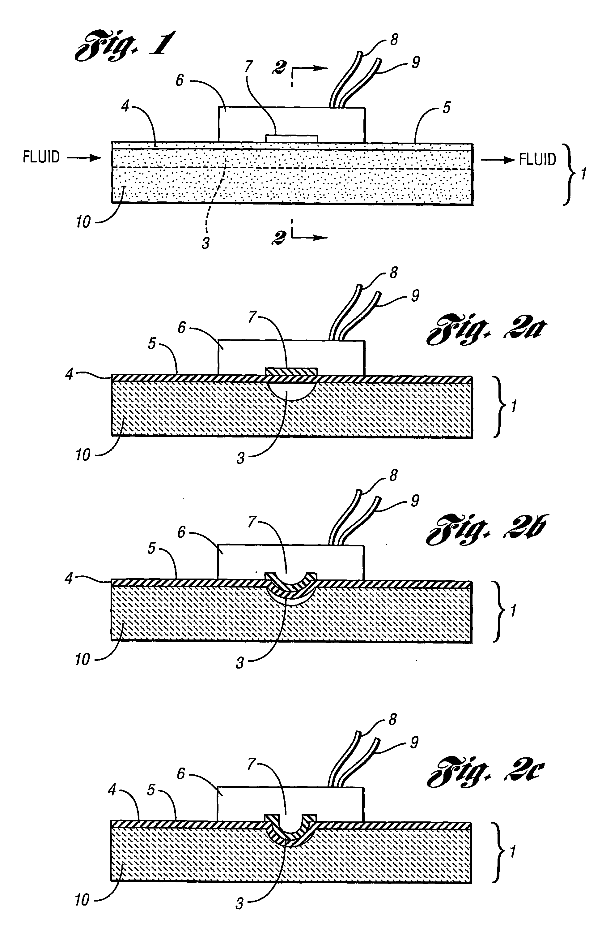
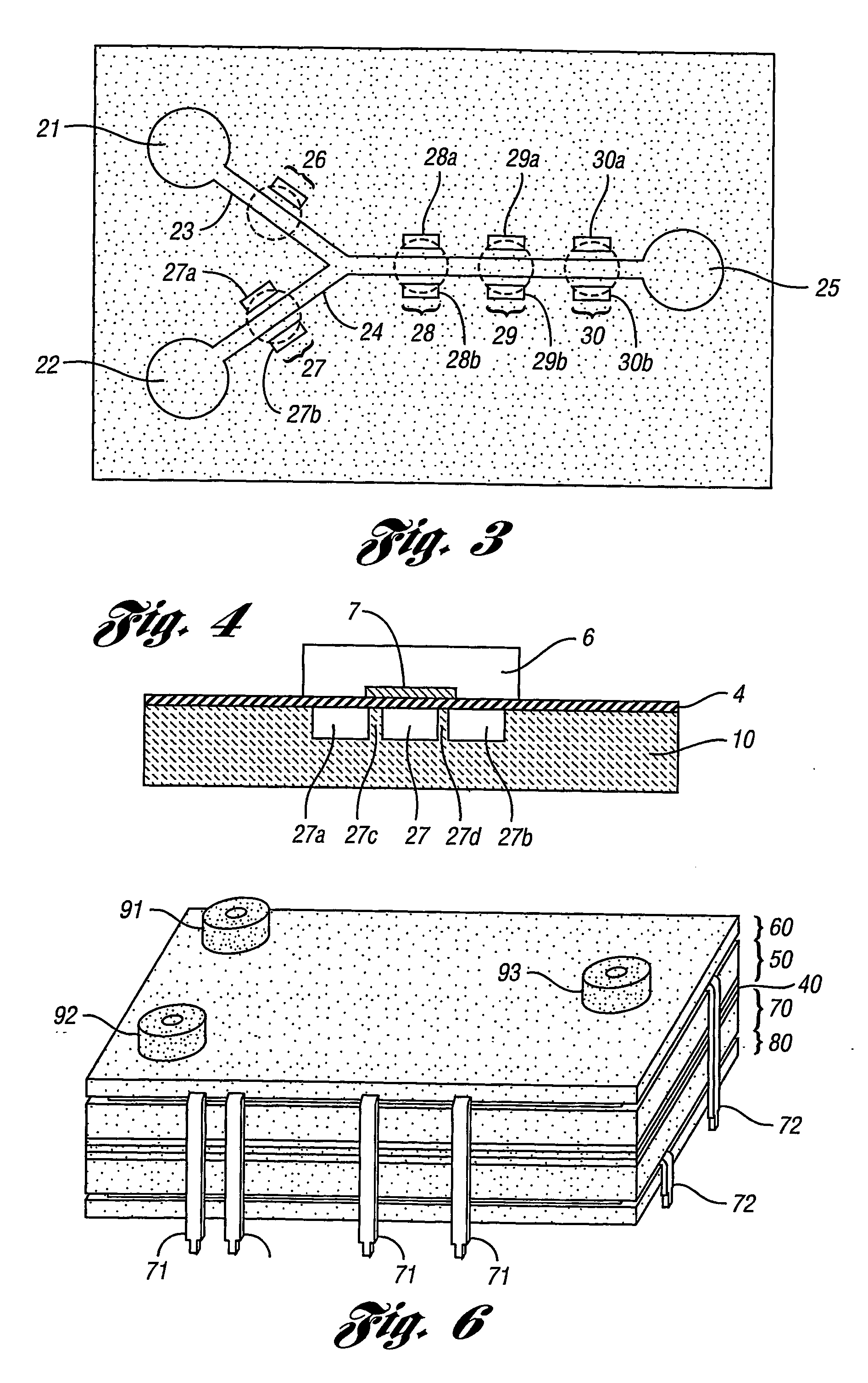
[0064] A microfluidic device is fabricated of PDMS (SYLGARD® 184) with active portions located below a commercial Braille display having 8-dot cells, the protrusions of which are approximately 1 mm in diameter, at spacings of 2.5 mm center-to-center in each cell, with an intercell distance of 3.2 mm. Each protrusion can protrude 1.5 mm from the surface of the display when activated. The elastomeric PDMS device channels have a relatively thin 100-200 μm bottom PDMS membrane, which rests upon the Braille display. The microfluidic device has a common observation channel and two valved supply channels, and is used to study Braille display actuated valving. The valves are constructed as described earlier with voids adjacent the active portions, and located on the microfluidic device so as to be below dimples on a commercial Braille display. One inlet channel is supplied with a solution of fluorescent dye from an inlet reservoir, while the other inlet reservoir contains no dye. The respec...

example 2

[0066] Photoplotted films were ordered from CAD / Art Services, Inc. (Poway, Calif.). Four-inch double-sided polished borosilicate glass wafers (thickness=200 μm) were from Plan Optik GmbH (Elsoff, Germany), 48 mm×65 mm borosilicate cover glasses (thickness=160 μm) from Fisher Scientific, negative photoresist SU-8 50 from MicroChem Corp. (Newton, Mass.), and PDMS (Sylgard 184) from Dow Corning (Midland, Mich.). Photoresist was exposed by a transilluminator (FB-TIV-816A, Fisher Scientific) with six replaced fluorescent blacklight lamps (TL-D15W / 08, Philips), and a PLA-501FA mask aligner by Canon U.S.A., Inc. (Lake Success, N.Y.). Oxidation was performed using a plasma etcher (Plasma Prep II; Structure Probe Inc., West Chester, Pa.). A Braille display DotView DV-1 was obtained from KGS Corp. (Saitama, Japan). Phosphate-buffered saline (PBS) was obtained from Fisher Scientific.

[0067] Photomasks of microchannels (width: 10 μm˜400 μm) were produced by photoplotting at 20,000 dpi to form a...

example 3

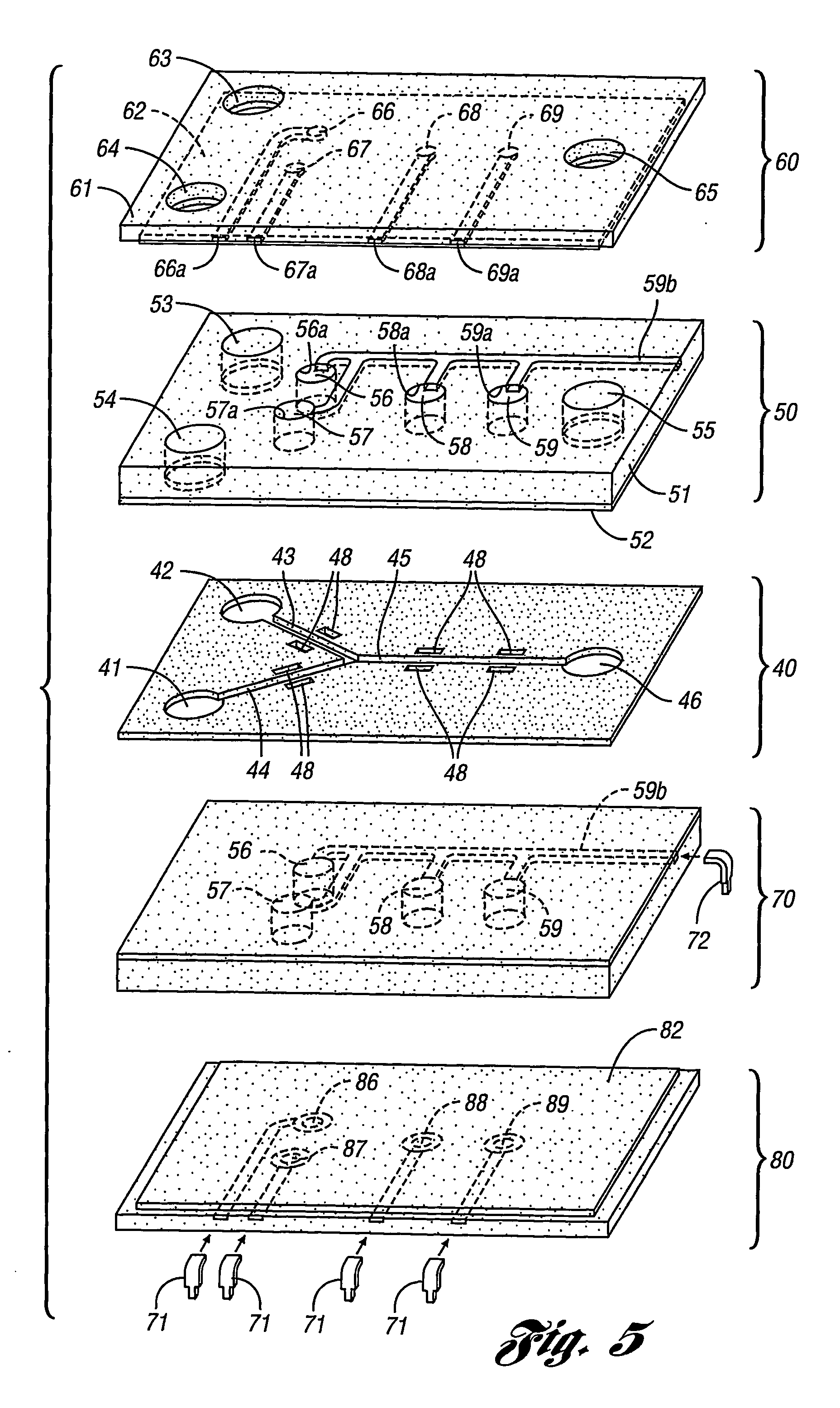
[0070] Each silicone chip is a multilayer assembly of poly(dimethylsiloxane) (PDMS). The bottom layer is formed at a thickness of 120 μm by spin coating a 1:10 (curing agent:base) ratio of prepolymer (Sylgard 184, Dow-Corning) onto a silanized glass wafer at 200 rpm for 4 minutes. A Si master with positive relief structure is made of photoresist (SU-8, MicroChem) defined through backside diffused-light photolithography as described in Example 2. Prepolymer (1:10 ratio) is cast against the positive relief features to form a ˜1 mm middle layer. The resultant negative replica formed channels when sealed by the bottom layer. Holes are punched by sharpened 14-gauge blunt needles through the middle layer towards the top layer. Prepolymer of ratios 1:10 and then 1:20 is successively poured on machined brass molds so that the ceiling of the top layer was richer in prepolymer base, providing a better sealant for future injections by needles. All three cured layers attached firmly together af...


PUM

PropertyMeasurementUnit
thicknessaaaaaaaaaa
depthaaaaaaaaaa
heightaaaaaaaaaa

Abstract

Microfluidic devices having active features such as valves, peristaltic pumps, and mixing portions are fabricated to have a thin elastomeric membrane over the active features. The active features are activated by a tactile actuator external to the membrane, for example, a commercial Braille display. The display may be computer controlled, for example by simple text editor software, to activate individual Braille protrusions or a plurality of protrusions to actuate the active portions of the microfluidic device. Integral devices can incorporate the tactile actuators in a single device, but still external to the membrane.

Description

BACKGROUND OF THE INVENTION [0001] 1. Field of the Invention [0002] The present invention is directed to active microfluidic devices. [0003] 2. Background Art [0004] Microfluidic devices are miniature devices generally containing a plurality of interconnected microchannels, reservoirs, etc., of very small size. Microchannels may commonly have width and height dimensions of 10 μm to 300 μm, for example, although smaller and larger dimensions are possible as well. As an aim to miniaturization and cost reduction, it is desirable to construct “lab on a chip” devices which contain all necessary functions with the exception of external fluid supply, and electrical, magnetic, or pneumatic energy supply when appropriate. [0005] Examples of microfluidic devices include micro flow cytometers as disclosed in K. Kurabayashi, et al., “Flow Cytometers and Detection System of Lesser Size,” published PCT Application No. WO 03 / 008937 A2 and motile sperm sorters as disclosed in S. Takayama, et al., “...

Claims


Application Information

Patent Timeline
Patent Type & Authority Applications(United States)
IPC IPC(8): C12M3/00B01L3/00B81B3/00C12M1/00C12N5/07F04B43/04G06FG06F3/00G06F3/14
CPCB01J2219/00396B01J2219/00891B01L3/50273B01L3/502738B01L2200/10B01L2200/12B01L2200/143B01L2300/025B01L2300/044B01L2300/0816B01L2300/0867B01L2300/0877B01L2300/0887B01L2300/123B01L2400/0481B01L2400/0638B01L2400/0655C12M23/16F16K99/0001F16K99/0026F16K99/0048F16K2099/0074F16K2099/0078F16K2099/008F16K2099/0084G09B23/12G06F3/14G06F3/00
Inventor TAKAYAMA, SHUICHIZHU, XIAOYUEGU, WEISMITH, GARY DANIELHEO, YUNSEOKCHO, BRENDA S.FUTAI, NOBUYUKI
Owner RGT UNIV OF MICHIGAN
Why Eureka
Try Eureka