

Semiconductor substrate, semiconductor device, light emitting diode and producing method therefor
a semiconductor and substrate technology, applied in the direction of chemically reactive gas growth, crystal growth process, polycrystalline material growth, etc., can solve the problems of difficult preparing large-sized substrates, low mechanical strength, and high cost of compound semiconductor substrates, and achieve the effect of ensuring economical properties
- Summary
- Abstract
- Description
- Claims
- Application Information
AI Technical Summary
Benefits of technology
Problems solved by technology
Method used
Image

Examples
example 1
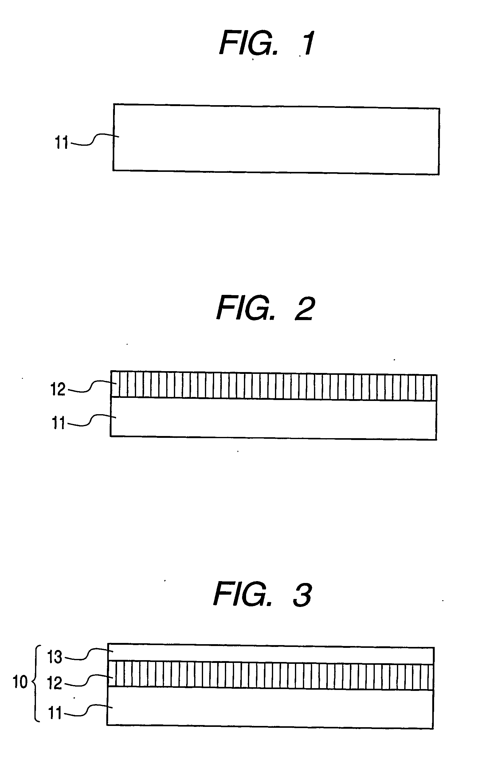
[0068] At first, a P-type Ge substrate 11 of a specific resistivity of 0.01 Ω·cm was prepared. Then the Ge substrate 11 was anodized in an anodizing solution to form a porous Ge layer as a separating layer 12. The anodizing conditions were as follows:
[0069] current density: 6 (mA / cm2)
[0070] anodizing solution: HF:H2O:C2H5OH=1:1:1
[0071] period: 11 (minutes)
[0072] thickness of porous Ge: 12 (μm).
[0073] The current density and the concentration of the anodizing solution can be suitably varied according to the thickness and the structure of the separating layer (porous Ge layer) 12 to be formed. The current density is preferably within a range of 0.5 to 700 mA / cm2, and the concentration of the anodizing solution is preferably within a range of 1:10:10 to 1:0:0.
[0074] The porous Ge layer is effective as a relaxing layer for forming an epitaxial GaAs layer of a high quality thereon and as a separating layer.
[0075] The anodizing solution can be a solution containing HF, and may be f...
example 2
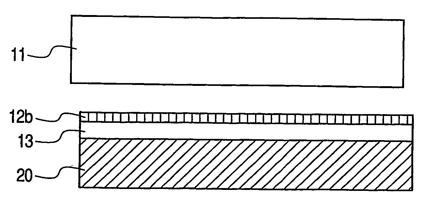
[0095] This example is a development of the example 1 and provides a method for producing a semiconductor device. At first, a porous Ge layer 22 is formed on a Ge substrate 21, in the same manner as shown in FIGS. 1 and 2 in the example 1.
[0096] Then, as shown in FIG. 8, an n-GaAs layer 23 is epitaxially grown on the porous Ge layer 22, and then an n-AlGaAs layer 24 as an n-clad layer, a GaAs layer 25 as an active layer and an AlGaAs layer 26 as a p-clad layer are epitaxially grown in succession on the n-GaAs layer 23 to form a laser structure 50.
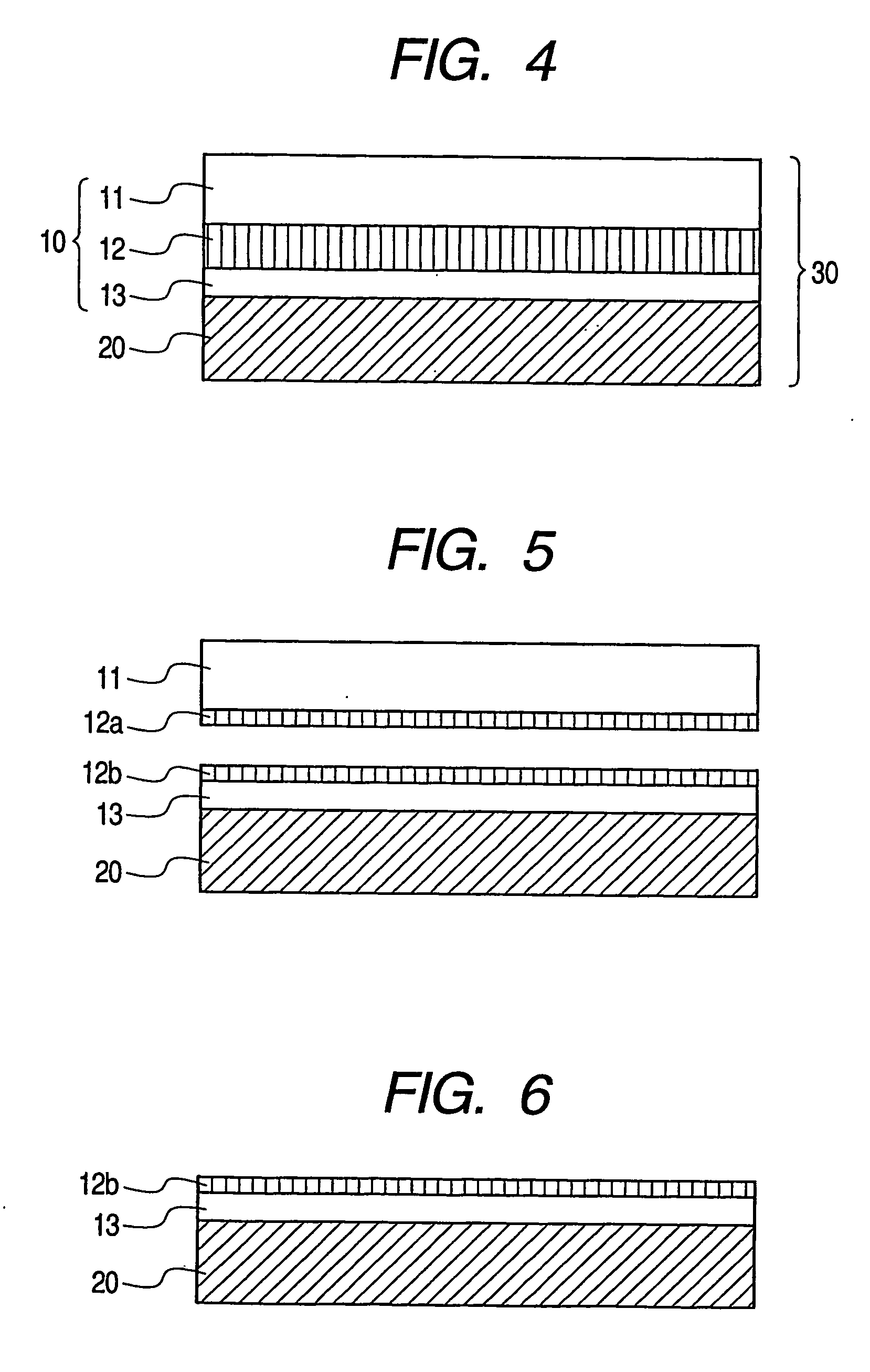
[0097] Then, in the same manner as shown in FIG. 4 of the example 1, the surface of the p-AlGaAs layer 26 of the laser structure 50 is superposed and bonded with a surface of a separately prepared substrate 20. Though not illustrated, an electrode is formed on the substrate 20 and can be electrically connected with the p-AlGaAs layer 26. The porous Ge layer, having an enormously large surface area, has a getter function of eliminating imp...
example 3
[0101] In an example 3, at first two porous germanium layers 102, 103 are formed by anodizing on a germanium substrate 101 as shown in FIG. 10. As the porous layer by anodizing is formed from the surface, a porous germanium layer 103 with a lower porosity is at first formed, and then a porous germanium layer 102 with a larger porosity is formed. This process allows to facilitate a next step of closing pores, present on the surface prior to epitaxial growth, and to smoothly separate the germanium substrate 101 in a later step.
[0102] Then a high-temperature hydrogen annealing and a CVD process utilizing GeH4, GeCl4 etc. as the raw material gas close the pores present on the surface of the porous germanium layer to form a satisfactory crystalline surface on the surface of the porous germanium, and a single crystal germanium layer 104, an n-GaAs layer 105, an n-AlxGa1-xAs layer 106, an n-AlyGa1-yAs layer 107, an n-AlxGa1-xAs layer 108, and an n-GaAs layer 109 (y<x) are epitaxially grow...
PUM
 Abstract
Description
Claims
Application Information