Semiconductor device manufacturing device

a manufacturing device and semiconductor technology, applied in semiconductor/solid-state device manufacturing, basic electric elements, electric devices, etc., can solve the problems of low dielectric constant film, copper presents difficulties in patterning by dry etching, and resist removal step is liable to damage, so as to achieve small alignment differences

Inactive Publication Date: 2006-07-27
SONY CORP
View PDF2 Cites 20 Cited by
  • Summary
  • Abstract
  • Description
  • Claims
  • Application Information

AI Technical Summary

Benefits of technology

[0068] The second aspect of the present invention offers the following advantages. When the resist mask having the connecting hole pattern is formed in step (c), the underlying layer is almost flat, and this makes it possible to form the resist mask having the accurate connecting hole. In this way it is possible to make the fine connecting hole in a stable manner without aggravating the shape of the wiring groove. Thus it is possible to obtain the good via contact characteristics.
[0069] Moreover, the patterning of the wiring groove is performed after the patterning of the connecting hole, and this avoids the indirect mask alignment of the upper layer wiring and the connecting hole. Therefore, it is possible to form the multi-layer wiring having a small alignment difference.

Problems solved by technology

The recent advance in miniaturized and highly integrated semiconductor devices pose a serious problem with delay of electric signals resulting from the time constant of wiring.
Unfortunately, copper presents difficulties in patterning by dry etching unlike the conventional metallic material (such as aluminum) used for multi-layer wiring.
First, the low dielectric constant film is liable to damage in the step of removing the resist, because it is similar in composition to the resist used for patterning.
Second, the process should be applicable to the borderless structure which does not allow alignment margin for the wiring and the connecting hole.
Second, the resist mask 12 is formed on the step several times. This presents difficulties in forming fine patterns accurately.
However, forming a fine resist pattern for the design rule of 0.10 μm on a local step slightly lower than 200 nm is much more difficult than forming it on a flat surface on account of resist mask spreading and uncontrollable line width.
This results in variation in depth of field, which in turn deteriorates the shape of the resist at the time of exposure or deteriorates the shape of the second mask 11 when the connecting hole is made by etching on the BARC film.
As compared with the ordinary process in which the pattern of the connecting hole is made first, the above-mentioned process causes more incomplete alignment for the upper wiring and the connecting hole.
Unfortunately, the metal film is almost opaque to light (with a wavelength of 200 to 1000 nm) used for mask alignment.
Therefore, if the metal film is formed over the entire surface, it makes it impossible to perform alignment with light of ordinary wave lengths or alignment by image processing in the exposure step.

Method used


Image

  • Semiconductor device manufacturing device
  • Semiconductor device manufacturing device
  • Semiconductor device manufacturing device

Examples


embodiment 1

[0085] This embodiment demonstrates the process for production of a semiconductor device according to the first aspect of the present invention. FIGS. 1 to 3 are sectional views each showing the steps of forming the dual damascene structure on the semiconductor substrate by the process employed in this embodiment. Identical symbols are used to indicate those parts in FIGS. 1 to 3 and those parts in FIG. 7 to 9, which function in the same way. This applies also to FIGS. 4 to 6.

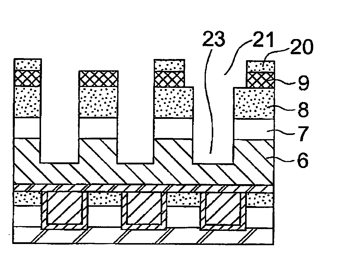
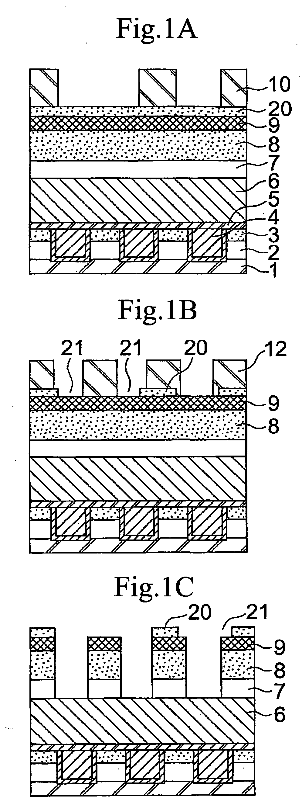
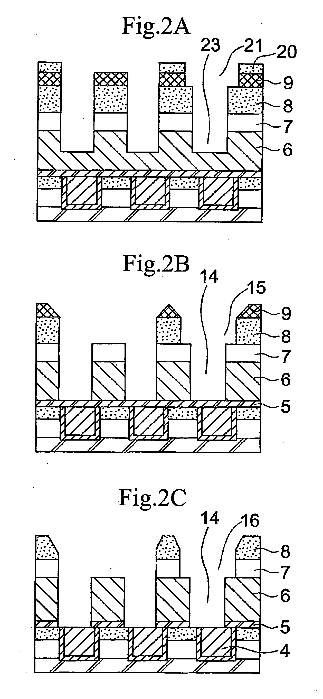
[0086] The process of this embodiment starts with the first step shown in FIG. 1A. A substrate (not shown) is coated with an underlying insulating film 1 by deposition. On the underlying insulating film 1 is formed an interlayer insulating film which is composed of an organic film 2 and a silicon oxide (SiO2) film 3. In the interlayer insulating film is formed a buried wiring 4 of copper (Cu) film, which is 250 nm thick.

[0087] On the Cu wiring 4 is formed a silicon carbide (SiC) film 5, 50 nm thick, as an oxi...

embodiment 2

[0137] This embodiment demonstrates the process for production of a semiconductor device according to the second aspect of the present invention. FIGS. 4 to 6 are sectional views each showing the steps of forming the dual damascene structure by the method employed in this embodiment.

[0138] As in Embodiment 1, the process of this embodiment starts with the first step shown in FIG. 4A. A substrate (not shown) is coated with an underlying insulating film 1 by deposition. On the underlying insulating film 1 is formed an interlayer insulating film which is composed of an organic film 2 and a silicon oxide (SiO2) film 3. In the interlayer insulating film is formed a buried wiring 4 of copper (Cu) film.

[0139] On the buried wiring 4 of Cu film is formed a silicon carbide (SiC) film 5, 50 nm thick, as an oxidation preventing film. Then, a carbon-containing silicon oxide (SiOC) film 6, 400 nm thick, is formed. Further, a polyaryl ether (PAE) film 7, 200 nm thick, is formed, which is an orga...


PUM


Abstract

A process for production of a semiconductor device having a multi-layer wiring of dual damascene structure in a low-dielectric constant interlayer insulating film. The process consists of the following steps. A first insulating film (6) and a second insulating film (7) are formed. A first to third mask forming layers (8), (9), and (20) are formed. The third mask forming layer is patterned so as to form the third mask for the wiring groove pattern. A resist mask of the connecting hole pattern is formed on the second mask forming layer including the third mask. The third mask and the second and first mask forming layers are etched, and the second insulating film is etched. The second mask of the wiring groove pattern is formed by using the third mask, and the connecting hole is made to the middle of the first insulating film. The first mask forming layer is etched by using the second mask, and the first mask of the wiring groove pattern is formed, and the first insulating film remaining at the bottom of the connecting hole is etched so as to make the connecting hole. The wiring groove is formed in the second insulating film by using the first or second mask.

Description

TECHNICAL FIELD [0001] The present invention relates to a process for production of a semiconductor device having the multi-layer wiring of dual damascene structure in the interlayer insulating film having a low dielectric constant. More particularly, the present invention relates to a process for production of a semiconductor device of dual damascene structure in good shape. BACKGROUND ART [0002] The recent advance in miniaturized and highly integrated semiconductor devices pose a serious problem with delay of electric signals resulting from the time constant of wiring. One way to address this problem is to form the conductive layer for the multi-layer wiring from low-resistant copper (Cu) in place of aluminum (Al) alloy. [0003] Unfortunately, copper presents difficulties in patterning by dry etching unlike the conventional metallic material (such as aluminum) used for multi-layer wiring. Therefore, the multi-layer wiring of copper is formed usually by the damascene process, which ...

Claims


Application Information

Patent Timeline
Patent Type & Authority Applications(United States)
IPC IPC(8): H01L21/4763H01L21/3065H01L21/768
CPCH01L21/76811H01L21/76835H01L21/76813H01L21/3065H01L21/768
Inventor KANAMURA, RYUICHI
Owner SONY CORP
Why Eureka
Try Eureka