Semiconductor device

a technology of semiconductor chips and semiconductor chips, applied in semiconductor devices, semiconductor/solid-state device details, electrical apparatus, etc., can solve the problems of easy degradation of the region in the vicinity of the front surface, the inability of the semiconductor chip to suitably follow the thermal expansion or thermal shrinkage of etc., to achieve the reduction of the linear expansion coefficient between the substrate of the semiconductor chip and the printed circuit board, the effect of improving heat resistan

Inactive Publication Date: 2006-08-03
RENESAS ELECTRONICS CORP
View PDF7 Cites 20 Cited by
  • Summary
  • Abstract
  • Description
  • Claims
  • Application Information

AI Technical Summary

Benefits of technology

[0010] The semiconductor device according to the above-described aspect of the present invention is configured to provide the front surface electrode of the semiconductor chip so as to be opposed to the insulating substrate and the semiconductor chip is flip-bonded to the insulating substrate. Further, the insulating substrate has the multiple-layered interconnects, and the surface electrode is electrically connected to the external mounting terminal through the multiple-layered interconnects in the multiple-layered interconnect layer. Consequently, a conduction path having a lower resistance passing through the multiple-layered interconnects can be ensured, even if a configuration that the element formation surface of the semiconductor chip is opposed to the insulating substrate, instead of being opposed to the printed circuit board, is employed. Further, sufficiently larger electric current can be supplied to the front surface electrode from the external mounting terminal.
[0011] In addition, since the front surface electrode of the semiconductor chip is disposed to be opposed to the chip-carrying region of the insulating substrate according to the above-described aspect of the present invention, the semiconductor chip is to be disposed on the printed circuit board in a position of being faced-up, while maintaining the condition that the back surface electrode is opposed to the printed circuit board. The difference in the linear expansion coefficient between the substrate of the semiconductor chip and the printed circuit board can be reduced by disposing the front surface electrode of the semiconductor chip so as to be opposed to the insulating substrate. Consequently, the stress concentration to the front surface electrode or the vicinity thereof can be inhibited, thereby providing an improved heat resistance in the condition of changing the temperature. Further, since a heat in the side of the front surface of the semiconductor chip is released to the outside of the chip from a conduction path along the above-described multiple-layered interconnect layer, the configuration providing an improved heat release characteristics can be obtained.
[0012] As such, the semiconductor according to the present invention is configured to ensure characteristics such as the applicability to applications utilizing larger electric current, lower resistance and the like with a simple configuration, as well as providing an improved heat release characteristics.
[0013] The semiconductor device according to the above aspect of the present invention may further have a configuration, in which an electroconductive through plug that provides a connection between a plurality of interconnects is provided on the insulating substrate. Having such configuration, heat release characteristics in the side of the element formation surface of the semiconductor chip can be further improved. The semiconductor device according to the above aspect of the present invention may further have a configuration, in which the through plug is provided right above the front surface electrode. This can provide a structure having the electric conductor of the insulating substrate, which is broadened from the right overhead of the front surface electrode of the semiconductor chip toward the circumference thereof, thereby providing a structural member that is an apparent radiation fin right above the front surface electrode. Consequently, further improved heat release characteristics in the side of the element formation surface of the semiconductor chip can be presented by the fin efficiency of the electric conductor in the insulating substrate.
[0014] According to the present invention, a technology providing an improvement in the durability in the condition of changing the temperature, while ensuring characteristics such as the applicability to applications utilizing larger electric current, lower resistance and the like can be achieved, by providing the flip-bonding of the semiconductor chip to the insulating substrate having the multiple-layered interconnect layer, providing the external mounting terminal in the side of the insulating substrate, on which the semiconductor chip is carried, and providing the electrical connection between the surface electrode of the semiconductor chip and the external mounting terminal through the multiple-layered interconnects provided in the insulating substrate.

Problems solved by technology

Since the linear expansion coefficient of the printed circuit board is larger than the linear expansion coefficient of the semiconductor chip, the semiconductor chip cannot suitably follow the thermal expansion or the thermal shrinkage of the printed circuit board in the case of the temperature variation after the mounting.
Since the stress concentrates in a region of the semiconductor chip in vicinity of the front surface electrode where a connection to the printed circuit board is made, a degradation is easily occurred in the region in vicinity of the front surface electrode.

Method used


Image

  • Semiconductor device
  • Semiconductor device
  • Semiconductor device

Examples


first embodiment

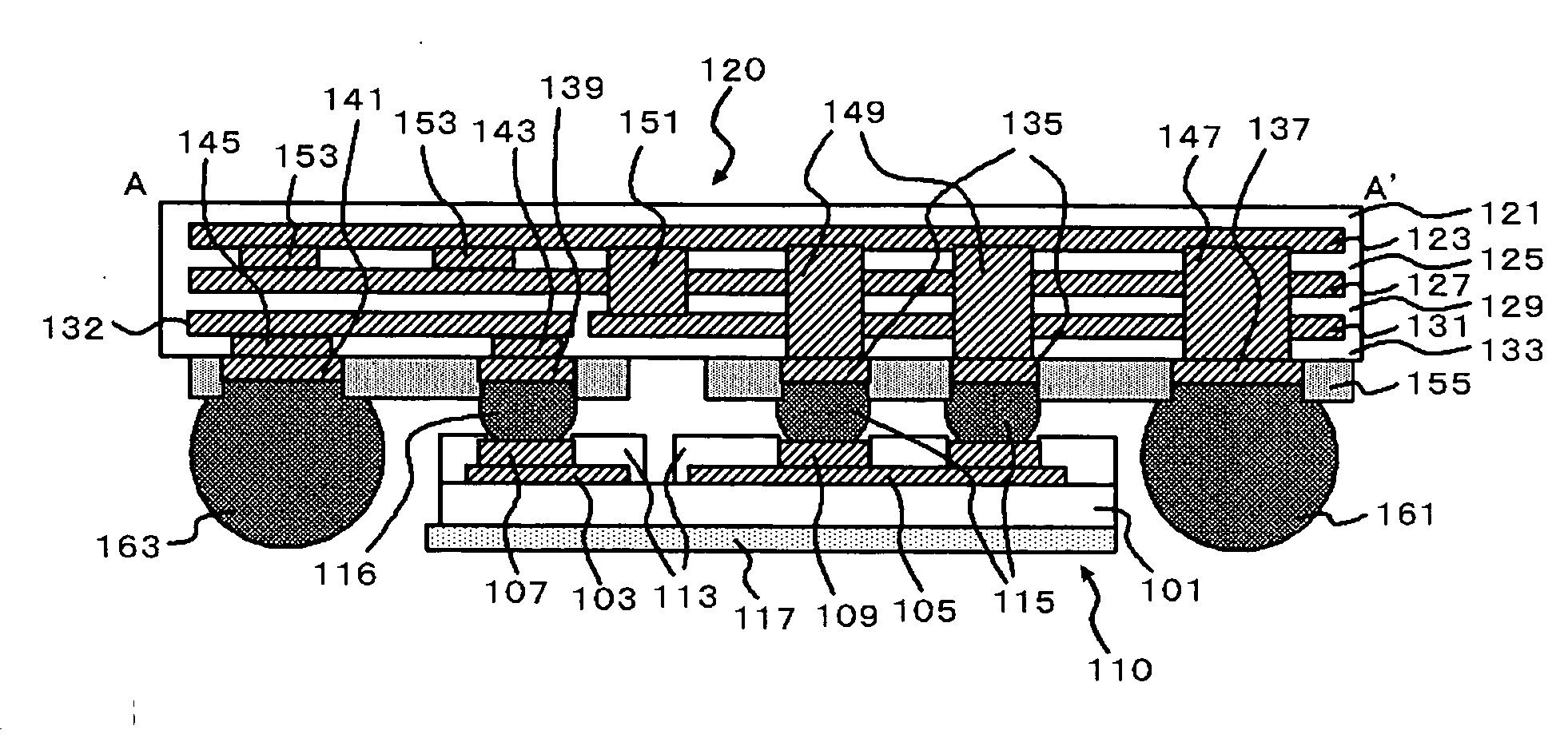
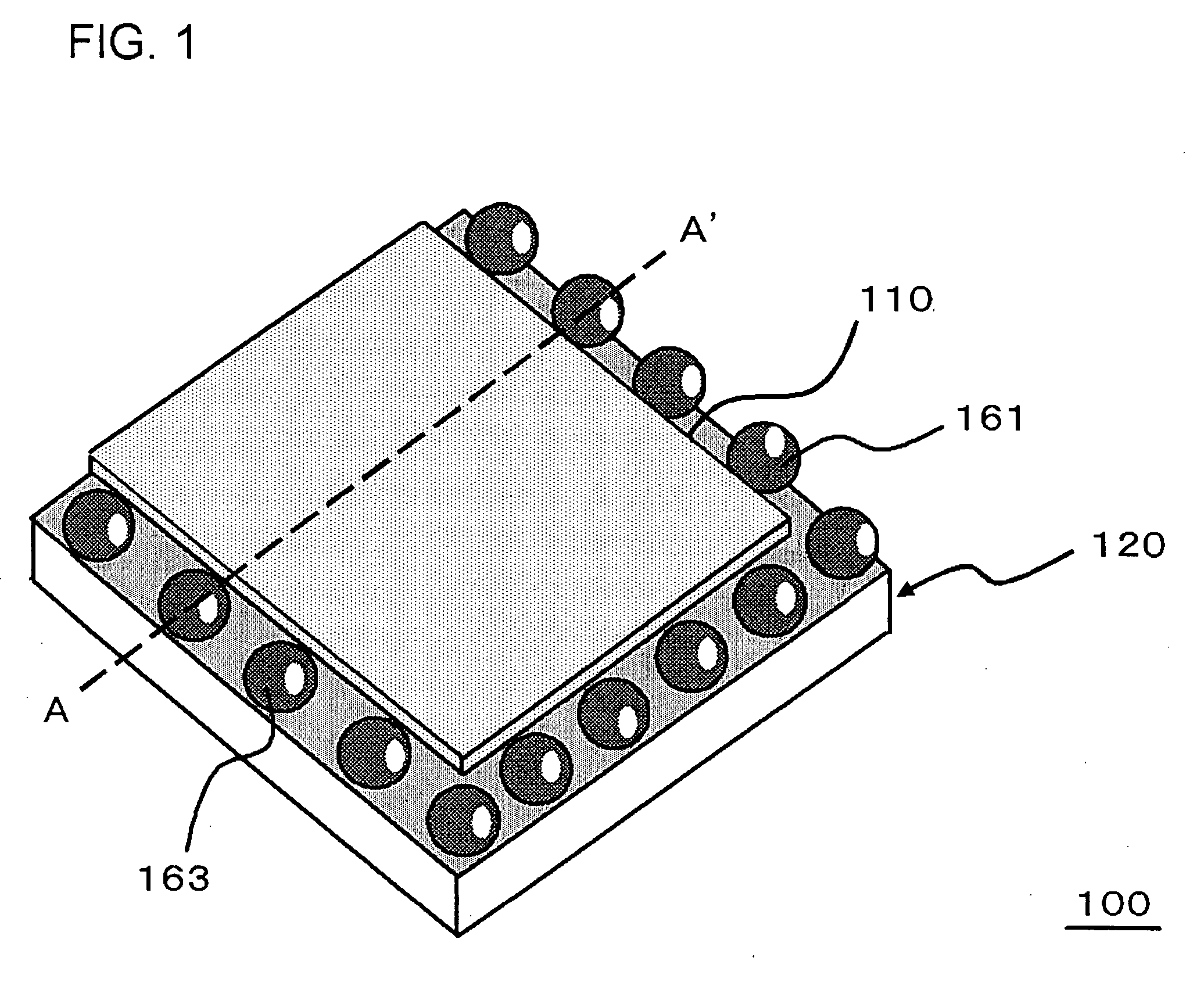
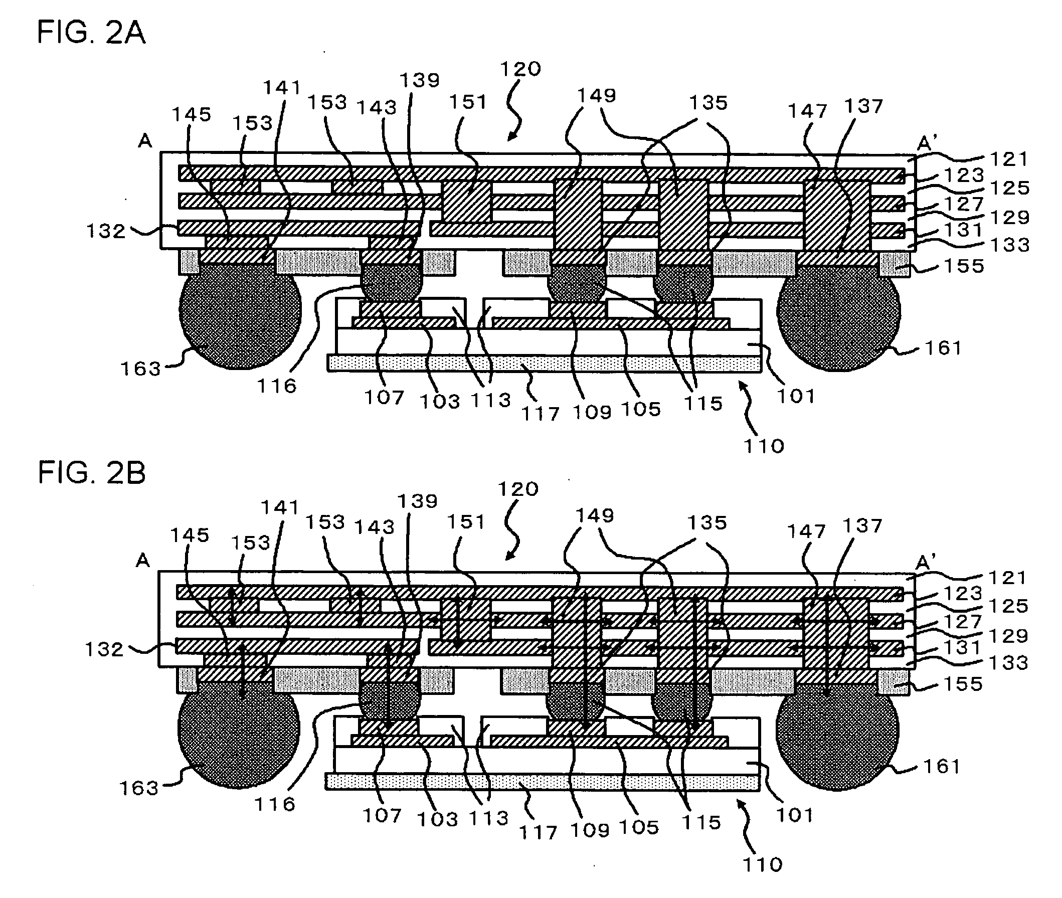
[0027]FIG. 1 is a perspective view, showing a configuration of a semiconductor device according to the present embodiment. FIG. 2A is a cross-sectional view of the semiconductor device along line A-A′ shown in FIG. 1. It should be noted that FIG. 2A shows the semiconductor device shown in FIG. 1 in a condition of being flipped.

[0028] The semiconductor device 100 shown in FIG. 1 and FIG. 2A includes an insulating substrate (ceramic multiple-layered interconnect substrate 120), a semiconductor chip (silicon chip 110) that is flip-bonded to a chip-carrying region of the ceramic multiple-layered interconnect substrate 120, and external mounting terminals (external connecting bumps 161), which are provided in the side that the silicon chip 110 of the ceramic multiple-layered interconnect substrate 120 is carried.

[0029] The silicon chip 110 includes front surface electrodes (second front surface electrodes 109) that are provided in the element formation surface of the silicon chip 110 a...

second embodiment

[0084] While the descriptions in first embodiment are related to the configuration, in which the external mounting terminal provided on the ceramic multiple-layered interconnect substrate 120 is the bump, and this bump is provided on the carrying surface for the silicon chip 110 in the ceramic multiple-layered interconnect substrate 120, The external mounting terminal may be provided in the side that the semiconductor chip of the ceramic multiple-layered interconnect substrate 120 is carried. For example, a conductive member may be exposed in the lower surface of the ceramic multiple-layered interconnect substrate 120, and the exposed surface may be utilized as an external mounting terminal.

[0085]FIG. 8 is a cross-sectional view, illustrating a configuration of a semiconductor device according to the present embodiment. FIG. 8 presents a view from the same direction as in FIG. 2A. A basic configuration of a semiconductor device 140 shown in FIG. 8 is similar to that of the semicond...


PUM

PropertyMeasurementUnit
thicknessaaaaaaaaaa
thicknessaaaaaaaaaa
thicknessaaaaaaaaaa

Abstract

A technology providing an improvement in the durability in the condition of changing the temperature, while ensuring characteristics such as the applicability to applications utilizing larger electric current, lower resistance and the like can be achieved. A semiconductor device 100 includes a ceramic multiple-layered interconnect substrate 120, a silicon chip 110 that is flip-bonded to a chip-carrying region of the ceramic multiple-layered interconnect substrate 120, and an external connecting bumps 161 and an external connecting bumps 163, which are provided in the side that the silicon chip 110 of the ceramic multiple-layered interconnect substrate 120 is carried. The silicon chip 110 includes a front surface electrode and a back surface electrode. The ceramic multiple-layered interconnect substrate 120 includes an interconnect layer composed of a conductive material, and the interconnect layer composes a multiple-layered interconnect layer provided on a front surface and in an interior of the ceramic multiple-layered interconnect substrate 120. The front surface electrode of the silicon chip is electrically connected to the external connecting bump 161 and the external connecting bump 163 through the multiple-layered interconnects in the multiple-layered interconnect layer.

Description

[0001] This application is based on Japanese patent application No. 2005-23,049, the content of which is incorporated hereinto by reference. BACKGROUND [0002] 1. Technical Field [0003] The present invention relates to a semiconductor device having a semiconductor chip bonded to a printed circuit board. [0004] 2. Related Art [0005] Compatibility to applications utilizing larger electric current, lower resistance and an improved heat release characteristics are required for semiconductor elements employed in electrical power applications. Since vertical metal oxide semiconductor (MOS) transistors or diodes among such semiconductor elements, for example, have configurations including electrodes on a front surface and a back surface of the semiconductor chip, it is necessary to respectively connect a front surface electrode and a back surface electrode to conductive materials of the mounting substrate, when it is to be mounted. Such type of technologies includes a technology described i...

Claims


Application Information

Patent Timeline
Patent Type & Authority Applications(United States)
IPC IPC(8): H01L23/48
CPCH01L23/13H01L23/49816H01L2924/13091H01L2924/10253H01L2924/15321H01L23/49822H01L2924/01079H01L2924/15311H01L2924/1532H01L2924/3011H01L2224/16225H01L2224/73253H01L2924/15153H01L2924/00H01L24/05H01L2224/05001H01L2224/05023H01L2224/05124H01L2224/05139H01L2224/05144H01L2224/05147H01L2224/05155H01L2224/05568H01L2224/32245H01L2924/00014H01L2924/12044H01L2924/15192H01L2224/05541H01L2224/05005H01L2224/05599
Inventor TANAKA, TAKEKAZUKOMATSU, IKUO
Owner RENESAS ELECTRONICS CORP
Why Eureka
Try Eureka