Magnetically directed self-assembly of molecular electronic junctions
- Summary
- Abstract
- Description
- Claims
- Application Information
AI Technical Summary
Benefits of technology
Problems solved by technology
Method used
Image
Examples
example 1
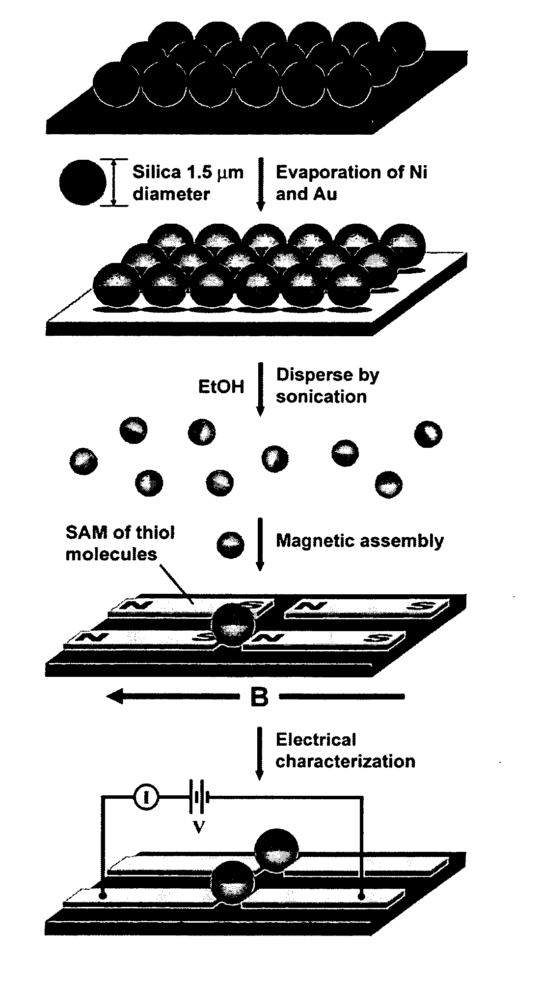
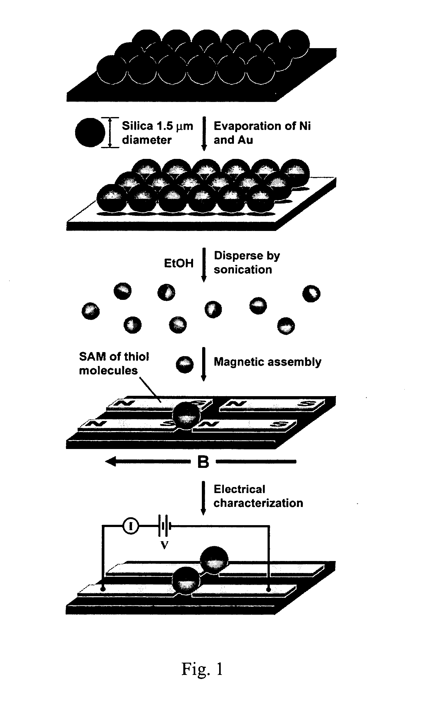
[0034] Formation of microspheres—2-D close-packed hexagonal monolayers of 1.5 micron silica beads were formed on 100 mm diameter silicon wafers by the slow evaporation of an ethanol dispersion of the colloid (Bangs Laboratories). Three prepared wafers were mounted simultaneously in an evaporative metallization chamber. 50 nm of nickel was deposited evenly on all wafers followed by 10 nm of gold. Following metallization, 100 mL of absolute ethanol was placed in a large beaker and the prepared wafers were added individually. Mild sonication for 20 min in a bath sonicator completely removed all metallized beads from the silicon surface creating a dark grey ethanol dispersion of the beads. All three wafers were stripped of their beads using the same dispersion. This concentrated “stock” solution was sonicated for another 20 minutes followed by removal of 0.5 mL of the dark dispersion. This aliquot was diluted to 100 mL with ethanol and again sonicated for 30 minutes. Approximately 10 mL...
example 2
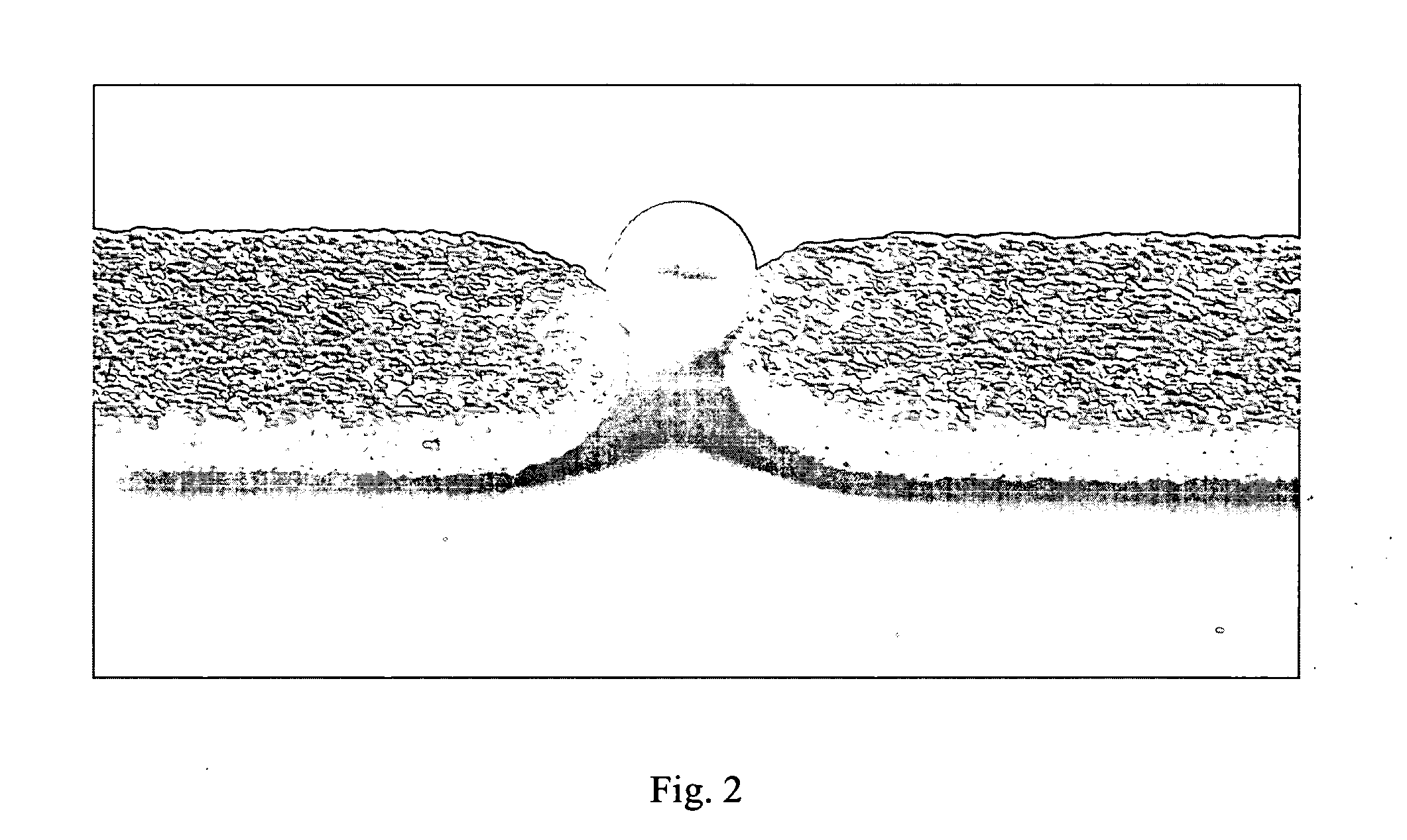
[0036] Magnetic self-assembly—The magnetic self-assembly of metallized colloid was conducted using arrays of high-aspect ratio devices composed of electroplated permalloy metal (Ni80Fe2O), the fabrication of which is described in Long et al., Adv. Mater., 16, 814 (2004). Features were encased in a thin layer of electroless gold to permit thiol monolayer formation on the surface of the electrodes. Each device incorporated a set of probe tips separated by a 1 μm gap where a locally intense magnetic field would direct entrapment of the microspheres. The specific combination of a 1 μm gap width and 1.5 μm diameter colloid was carefully chosen to prevent the spheres from fitting properly in the gaps. This forces electrical contact to be made further into the metallized region of the sphere where the deposited Ni / Au film is more continuous.
[0037] Approximately 3 ml of freshly sonicated microsphere dispersion was placed in a small test tube. The test tube was then placed in a 100 Gauss ma...
example 3
[0039] Current-voltage analysis—Room temperature current-voltage (I-V) analysis was conducted on non-functionalized microsphere junctions to determine the electrical properties of the metal-metal contacts generated using this technique. Improper bead orientation after trapping prevents electrical current through the device, however the majority of trapped beads display a preferred magnetic orientation which promotes electrical contact. Proper alignment of the colloid completes the circuit across the probe tips. I-V analysis of several such junctions revealed contact resistance from 100-600Ω, similar to reports of assembled metallic nanowires. The instrument compliance was set at 1 μA. The range of microsphere junction resistance is thought to be due to the exact positioning of the sphere and its manner of contact with the electrodes. Electrical contacts made near the edge of the metallized and silica regions were found to be of higher resistance due to lower thickness of the deposit...
PUM
| Property | Measurement | Unit |
|---|---|---|
| Length | aaaaa | aaaaa |
| Magnetic field | aaaaa | aaaaa |
| Electrical conductor | aaaaa | aaaaa |
Abstract
Description
Claims
Application Information
 - R&D
- Intellectual Property
- Life Sciences
- Materials
- Tech Scout
- Unparalleled Data Quality
- Higher Quality Content
- 60% Fewer Hallucinations
Browse by: Latest US Patents, China's latest patents, Technical Efficacy Thesaurus, Application Domain, Technology Topic, Popular Technical Reports.
© 2025 PatSnap. All rights reserved.Legal|Privacy policy|Modern Slavery Act Transparency Statement|Sitemap|About US| Contact US: help@patsnap.com


