Magnetic tunnel junction device and method of manufacturing the same

a tunnel junction and magnetic tunnel technology, applied in the direction of magnetic field-controlled resistors, digital storage, instruments, etc., can solve the problems of inability to read signals, signal loss in noise, and too small output voltage when operating margins are considered for the device to be employed for an actual memory device, etc., to achieve easy higher integration, increase the output voltage of the mtj device, and achieve greater magnetoresistance

Inactive Publication Date: 2006-08-10
JAPAN SCI & TECH CORP +1
View PDF7 Cites 21 Cited by
  • Summary
  • Abstract
  • Description
  • Claims
  • Application Information

AI Technical Summary

Benefits of technology

[0031] In accordance with the invention, an MTJ device having greater magnetoresistance than that of conventional MTJ devices can be obtained, so that the output voltage of the MTJ device can b

Problems solved by technology

With such characteristics, the output voltage when operation margins are taken into consideration is too small for the device to be employed for an actu

Method used


Image

  • Magnetic tunnel junction device and method of manufacturing the same
  • Magnetic tunnel junction device and method of manufacturing the same
  • Magnetic tunnel junction device and method of manufacturing the same

Examples


first embodiment

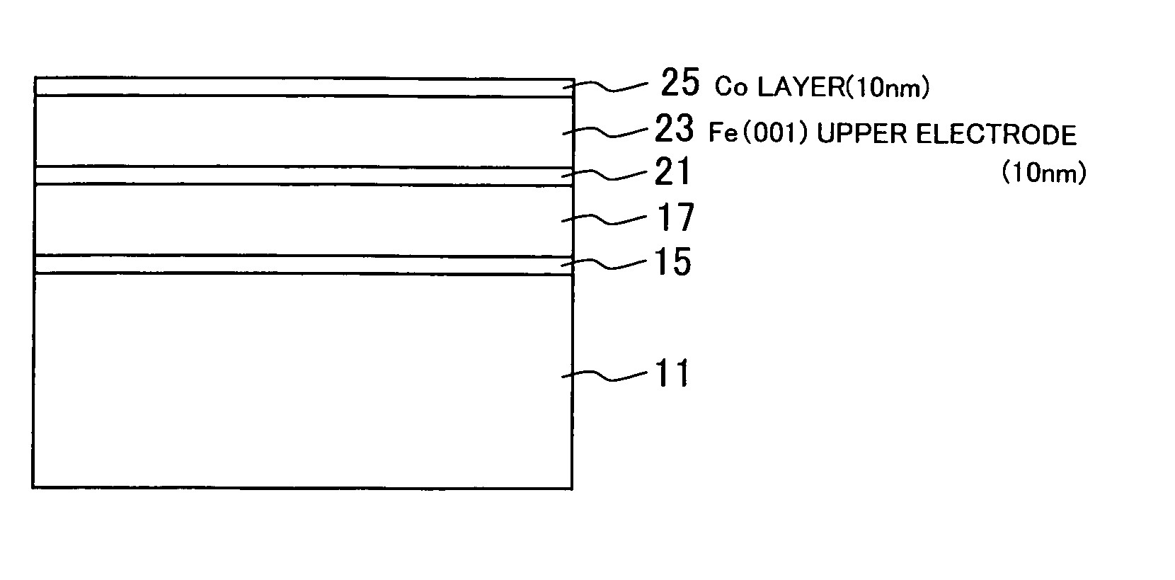
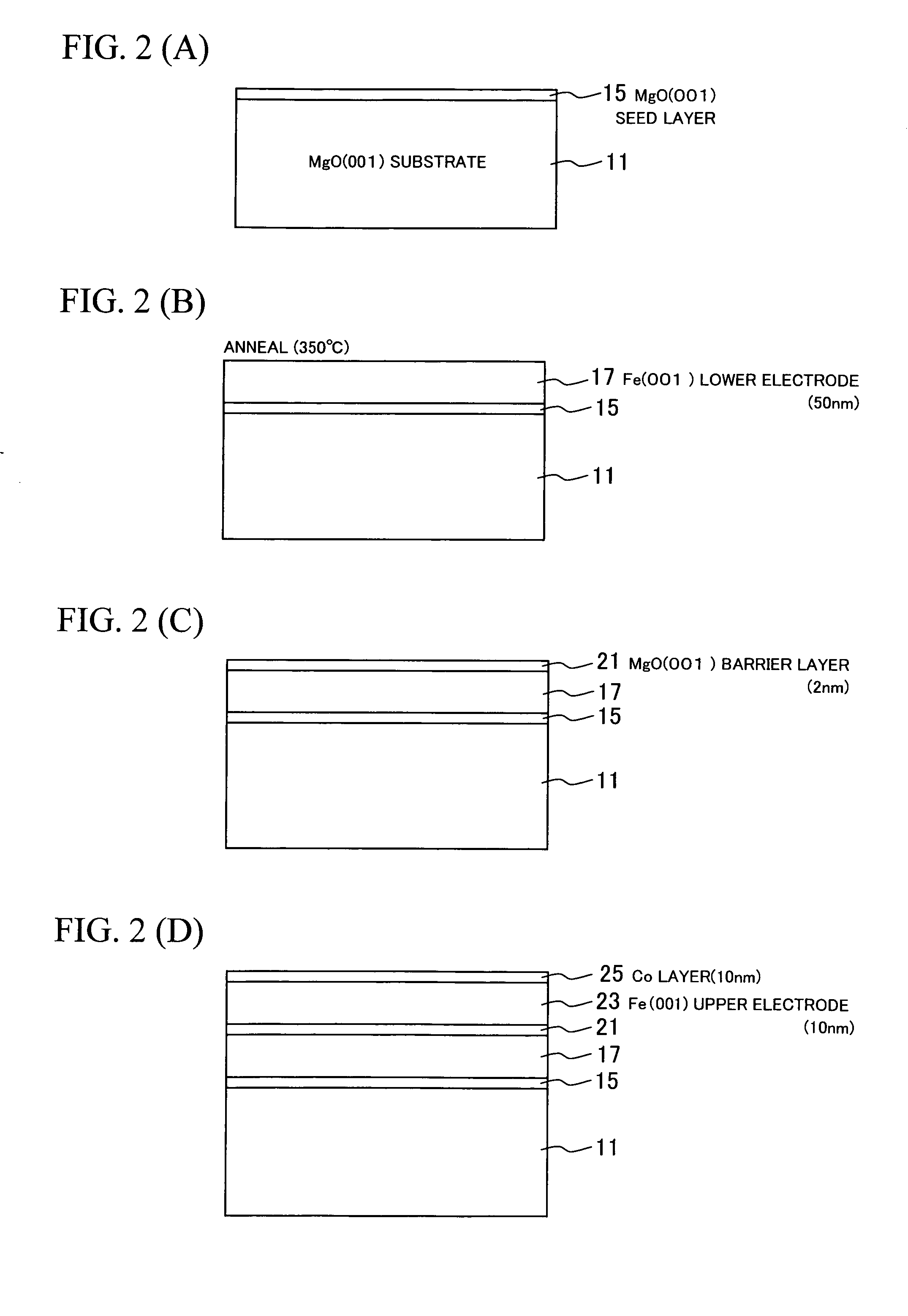
[0056] In the following, a MTJ device according to the invention and a method of manufacturing the same will be described with reference to the drawings. FIGS. 2(A) to 2(D) schematically show the method of manufacturing the MTJ device having the Fe (001) / MgO(001) / Fe(001) structure according to the embodiment (to be hereafter referred to as a “Fe(001) / MgO(001) / Fe(001) MTJ device”). Fe(001) refers to a ferromagnetic material with the BCC structure. First, a single-crystalline MgO(001) substrate 11 is prepared. In order to improve the morphology of the surface of the single-crystalline MgO(001) substrate 11, a MgO(001) seed layer 15 is grown by the molecular beam epitaxy (MBE) method. This is followed by the growth of an epitaxial Fe(001) lower electrode (first electrode) 17 with a thickness of 50 nm on the MgO(001) seed layer 15 at room temperature, as shown in FIG. 1(B). Annealing is then performed at 350° C. under ultrahigh vacuum (2×10⁻⁸ Pa). The electron-beam evaporation condition...

second embodiment

[0062] Hereafter, a magnetic tunnel junction device according to the invention and a method of manufacturing the same will be described. In the method of manufacturing a the Fe (001) / MgO (001) / Fe (001) MTJ device according to the present embodiment, MgO(001) is initially deposited in a poly-crystalline or amorphous state by sputtering or the like, and then an annealing process is performed such that a polycrystal in which the (001) crystal plane is oriented or a single crystal is obtained. The sputtering conditions were such that, for example, the temperature was room temperature (293K), a 2-inch φ MgO was used as a target, and sputtering was conducted in an Ar atmosphere. The acceleration power was 200 W and the growth rate was 0.008 nm / s. Because MgO deposited under these conditions is in an amorphous state, a crystallized MgO can be obtained by increasing the annealing temperature to 300° C. from room temperature and maintaining that temperature for a certain duration of time.

[00...

third embodiment

[0067] Hereafter, a MTJ device according to the invention will be described with reference to the drawings.

[0068] As already described above, output voltage can be increased by improving the bias voltage dependence or Vhalf of the MTJ device. In order to increase the Vhalf value of a MTJ device having an MgO (001) tunneling barrier, it is effective to lower the density of dislocation defects that exist at the interface between the MgO (001) tunnel barrier layer and the ferromagnetic metal electrode layer. FIG. 11(a) and (b) show cross-sectional transmission electron microscope images of the interface between a single-crystalline Fe (001) electrode layer and a single-crystalline MgO (001) tunnel barrier layer. In these images, dislocation defects can be observed at the interface. Such dislocation defects at the interface inevitably exist to a greater or smaller degree when the lattice constants (interatomic spacings) of the two layers are different. In the case of the interface betwe...


PUM


Abstract

The MR ratio of an MTJ device is increased. A single-crystalline MgO (001) substrate 11 is prepared, and then an epitaxial Fe (001) lower electrode (first electrode) 17 with a thickness of 50 nm is grown on a MgO (001) seed layer 15 at room temperature. Annealing is then performed in ultrahigh vacuum (2×10⁻⁸ Pa) at 350° C. A 2-nm thick MgO (001) barrier layer 21 is epitaxially grown on the Fe (001) lower electrode (first electrode) 17 at room temperature, using electron beam evaporation of MgO. A Fe (001) upper electrode (second electrode) 23 with a thickness of 10 nm is then grown on the MgO (001) barrier layer 21 at room temperature, which is successively followed by the deposition of a Co layer 21 with a thickness of 10 nm on the Fe (001) upper electrode (second electrode) 23. The Co layer 21 is used for realizing an antiparallel magnetization alignment by enhancing an exchange bias magnetic field of the upper electrode 23. Thereafter, the above-prepared sample is subjected to microfabrication so as to obtain a Fe (001)/MgO (001)/Fe (001) MTJ device. The density of dislocation defects that exist at the interface between one of the first or the second Fe (001) layer and the single-crystalline MgO (001) layer is not more than 25 to 50 defects/μm.

Description

BACKGROUND OF THE INVENTION [0001] 1. Field of the Invention [0002] The present invention relates to a magnetic tunnel junction device (MTJ device) and a method of manufacturing the same, and particularly to a magnetic tunnel junction device with a high magnetoresistance and a method of manufacturing the same. [0003] 2. Description of Related Art [0004] Magnetoresistive random access memories (MRAMs) refer to a large-scale integrated memory circuit that is expected to replace the currently widely used DRAM memories. Research and development of MRAM devices, which are fast and non-volatile memory devices, are being extensively carried out, and sample products of a 4 Mbit MRAM have actually been delivered. [0005]FIG. 7 shows the structure and operation principle of a magnetic tunnel junction device, which is the most important part of the MRAM. As shown in FIG. 7(A), a MTJ device comprises a tunneling junction structure in which a tunnel barrier made of an oxide is sandwiched between ...

Claims


Application Information

Patent Timeline
IPC IPC(8): G11C11/15
CPCG11C11/16H01L43/08H01L43/12H10N50/01H10N50/85H10N50/10
Inventor YUASA, SHINJI
Owner JAPAN SCI & TECH CORP
Why Eureka
Try Eureka