
Flash Memory Cell Arrays Having Dual Control Gates Per Memory Cell Charge Storage Element

a memory cell array and charge storage technology, applied in semiconductor devices, digital storage, instruments, etc., can solve the problems of difficult long-term data retention, inability to practically be thinned, and significant limitation of the continued shrinkage of the size of current non-volatile memory cell arrays, etc., to increase parasitic capacitance, increase the total coupling area, and increase the coupling ratio

Inactive Publication Date: 2006-08-10
SANDISK TECH LLC
View PDF73 Cites 20 Cited by
  • Summary
  • Abstract
  • Description
  • Claims
  • Application Information

AI Technical Summary

Benefits of technology

[0012] According to one primary aspect of the present invention, the memory cell array floating gates are individually coupled with at least two control gates, thereby to increase the total coupling area between floating and control gates without increasing the coupling area between the floating gate and the substrate, thus increasing the coupling ratio. In a NAND array, the control gates usually stacked on top of rows of floating gates are replaced by control gates positioned between the floating gates along the memory cell strings. The individual floating gates are then capacitively coupled through opposing sidewalls to two control gates, one on each side. The height of the floating gates is increased to increase the coupling area with these control gates. The total coupling area of an individual floating gate with the control gates is significantly increased independent of the coupling area between the floating gate and the substrate. This allows the control gate voltages to be significantly reduced but still results in increasing the voltage coupled to the floating gates to the values now used to control the memory cell channel through the gate dielectric having a given thickness.
[0013] In operation, the voltage of one row of floating gates is increased during their programming or reading by raising the voltage on the control gates on both sides of the row. A similar voltage rise of floating gates in adjacent rows is reduced, even though they are also coupled with one of these control gates whose voltage has been increased, by keeping the voltage low on control gates coupled with opposite sides of these adjacent rows of floating gates.
[0014] The positioning of control gates between floating gates along NAND memory cell strings also reduces the undesirable coupling between floating gates of adjacent cells because the electrically driven control gates tend to shield the electric field between the floating gates. Further, the control gates can be capacitively coupled to areas of the substrate between floating gates in order to boost the voltage of the substrate for certain operations such as inhibiting the programming of individual cells.
[0015] According to another primary aspect of the present invention, channel lengths of the individual transistors in the NAND strings having a given number of floating gate storage elements are significantly reduced, up to almost one-half existing lengths, by forming the floating gates using spacers having a dimension significantly less that the minimum resolution element size of the lithography being used in the process. Such spacers are formed over a layer of doped polysilicon or other conductive material, for example, of a first dielectric material along sides of strips of a second dielectric material. Once the second dielectric material is removed, the spacers of the first dielectric material form a mask through which the underlying conductive floating gate material is etched. The size of the floating gates and the spaces between them are reduced. The control gates are preferably provided between the smaller floating gates and operated in the same manner as described above. Smaller NAND memory cell strings result in more of them being formed in a given area, and a resulting increase in the density of data storage in a given size of memory cell array.

Problems solved by technology

A significant limitation on the continued shrinking of the size of current non-volatile memory cell arrays is the floating gate dielectric.
This cannot practically be made thinner than the approximately 70 Angstrom (7 nm) minimum thickness currently being used without resulting in leakage and difficulties in long term data retention.
This means that the voltages required to be coupled to the floating gates to control conduction in the memory cell channels below them cannot be reduced as the size of the various gates and distances between them are reduced.
Undesired coupling of voltages between the various gates increases as the distance between them decreases unless a compensating reduction in the voltage levels being used can be made.
Reduction of the coupling ratio is difficult to achieve in NAND arrays because of their stacked control and floating gate structures.
Another undesired effect of scaling is an increase in parasitic capacitances between conductive array elements, particularly between adjacent floating gates.
Errors in programming or in reading the state of one floating gate can, for example, be caused by the close proximity of the charge stored on the floating gate of an adjacent cell.
This coupling can create a significant number of errors in multi-state operation where the allowed range of threshold voltages of the floating gate transistor that is devoted to each state is very small.

Method used


Image

  • Flash Memory Cell Arrays Having Dual Control Gates Per Memory Cell Charge Storage Element
  • Flash Memory Cell Arrays Having Dual Control Gates Per Memory Cell Charge Storage Element
  • Flash Memory Cell Arrays Having Dual Control Gates Per Memory Cell Charge Storage Element

Examples


Embodiment Construction

Memory System

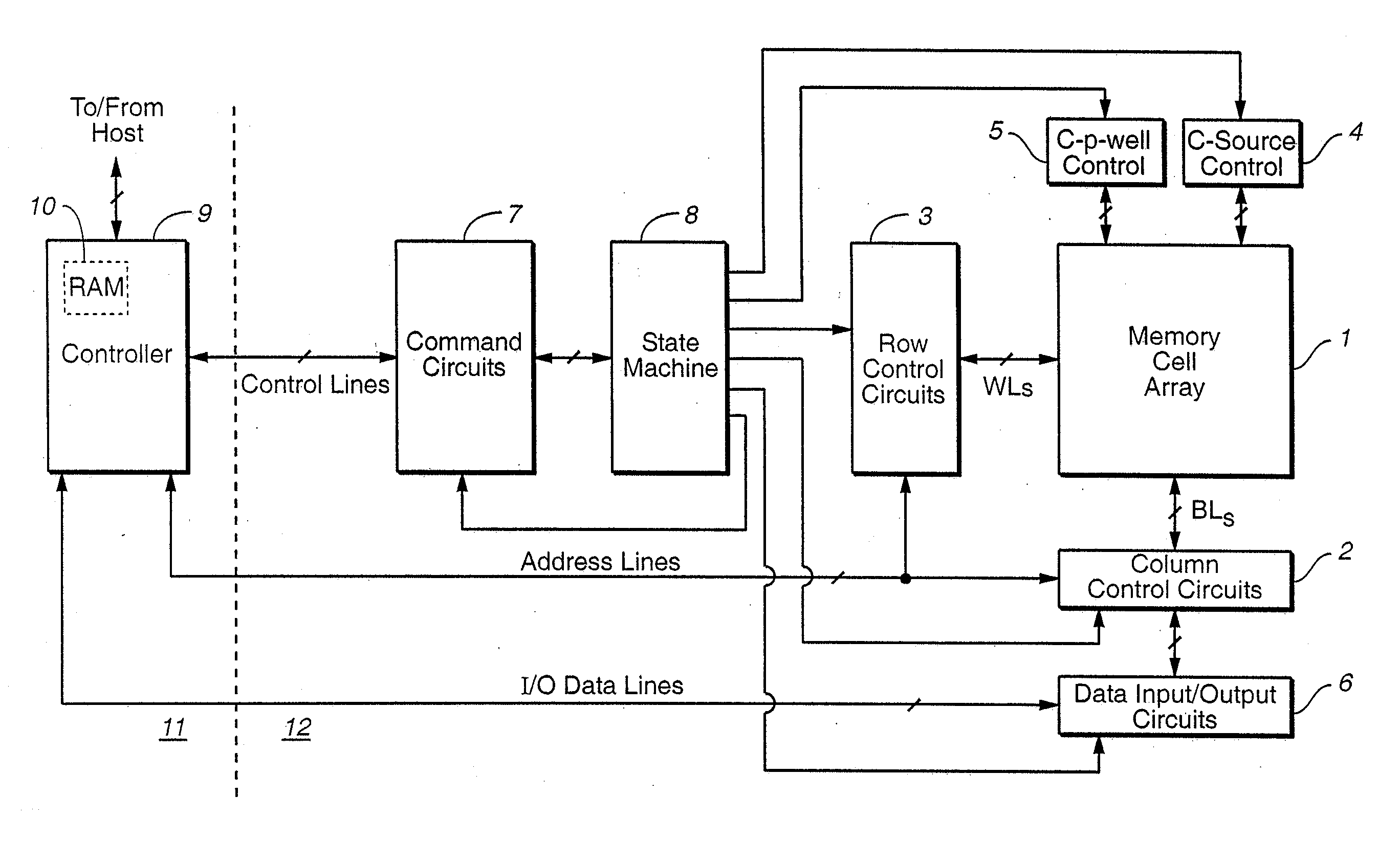
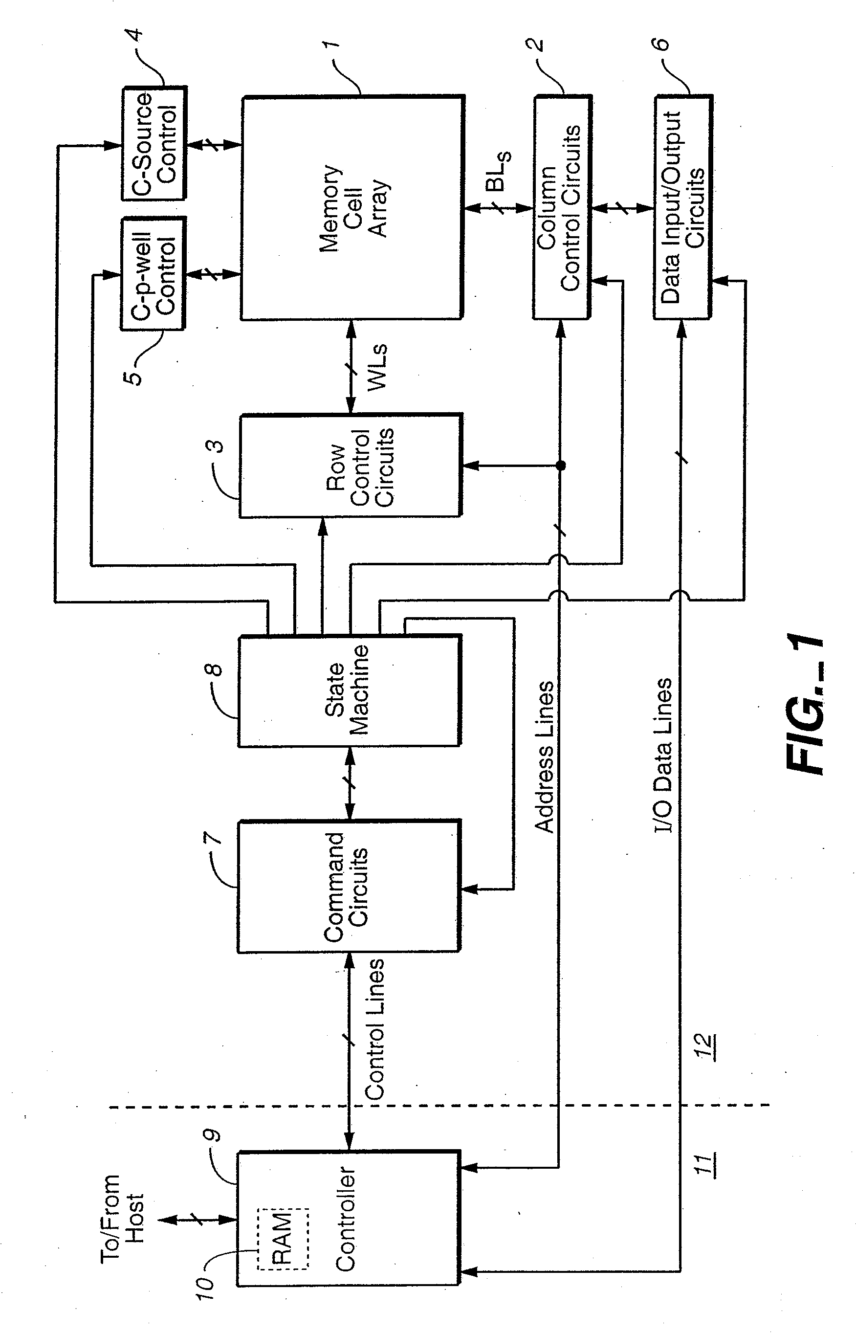
[0032] An example memory system in which the various aspects of the present invention may be implemented is illustrated by the block diagram of FIG. 1. A memory cell array 1 including a plurality of memory cells M arranged in a matrix is controlled by a column control circuit 2, a row control circuit 3, a c-source control circuit 4 and a c-p-well control circuit 5. The memory cell array 1 is, in this example, of the NAND type that is described above in the Background and in references incorporated herein by reference. A control circuit 2 is connected to bit lines (BL) of the memory cell array 1 for reading data stored in the memory cells (M), for determining a state of the memory cells (M) during a program operation, and for controlling potential levels of the bit lines (BL) to promote the programming or to inhibit the programming. The row control circuit 3 is connected to word lines (WL) to select one of the word lines (WL), to apply read voltages, to apply program v...


PUM


Abstract

A flash NAND type EEPROM system with individual ones of an array of charge storage elements, such as floating gates, being capacitively coupled with at least two control gate lines. The control gate lines are preferably positioned between floating gates to be coupled with sidewalls of floating gates. The memory cell coupling ratio is desirably increased, as a result. Both control gate lines on opposite sides of a selected row of floating gates are usually raised to the same voltage while the second control gate lines coupled to unselected rows of floating gates immediately adjacent and on opposite sides of the selected row are kept low. The control gate lines can also be capacitively coupled with the substrate in order to selectively raise its voltage in the region of selected floating gates. The length of the floating gates and the thicknesses of the control gate lines can be made less than the minimum resolution element of the process by forming an etch mask of spacers.

Description

CROSS REFERENCE TO RELATED APPLICATION [0001] This is a divisional of application Ser. No. 10 / 791,486, filed Mar. 1, 2004, which in turn is a divisional of application Ser. No. 10 / 282,747, filed Oct. 28, 2002, now U.S. Pat. No. 6,888,755, which applications are incorporated herein in their entirety by this reference.FIELD OF THE INVENTION [0002] This invention relates generally to non-volatile semiconductor memories of the flash EEPROM (Electrically Erasable and Programmable Read Only Memory) type, particularly to structures and methods of operating NAND types of memory cell arrays. BACKGROUND OF THE INVENTION [0003] There are many commercially successful non-volatile memory products being used today, particularly in the form of small form factor cards, which use an array of flash EEPROM cells. [0004] One popular flash EEPROM architecture utilizes a NAND array, wherein a large number of strings of memory cells are connected through one or more select transistors between individual b...

Claims


Application Information

Patent Timeline
Patent Type & Authority Applications(United States)
IPC IPC(8): G11C16/04H01L21/8247H01L27/115
CPCG11C16/0483H01L21/28273H01L27/115H01L27/11521H01L27/11524H01L29/42348H01L29/66825H01L29/7881H01L29/40114H10B69/00H10B41/30H10B41/35G11C16/04G11C11/34
Inventor HARARI, ELIYAHOU
Owner SANDISK TECH LLC
Learn More