
Semiconductor laser device

Inactive Publication Date: 2006-08-10
PANASONIC CORP
View PDF7 Cites 10 Cited by
  • Summary
  • Abstract
  • Description
  • Claims
  • Application Information

AI Technical Summary

Benefits of technology

[0023] The stated aim can be achieved by a semiconductor laser device including an optical resonator, the optical resonator including: an optical waveguide formed by laminating a cladding layer of a first conductivity type, an active layer, and a cladding layer of a second conductivity type in the stated order; and a pair of reflection planes formed by providing both a light emitting end face and an opposite end face of the optical waveguide with a reflection function, wherein a window region is formed in, of both end areas of the optical waveguide, at least an end area including the light emitting end face, by introduction of impurities. A length of the window region in the end area including the light emitting end face, measured in a resonator length direction, is set to prevent carriers which flow from a current injected region of the optical waveguide into the window region, from reaching the light emitting end face, or set to prevent carriers which are injected at an end of a gain region, from reaching the light emitting end face.
[0040] That is, by making the window region in the end area including the light emitting end face longer than the window region in the end area including the opposite end face, a sufficient length of the former window region can be ensured while maintaining high light output power.

Problems solved by technology

However, since this conventional technique simultaneously pursues desired horizontal divergence angle θ∥ and element resistance by reducing the ridge height, there may be cases where properties that are dependent on the ridge height cannot be optimized.
Thus, the semiconductor laser device according to the conventional technique has a problem that it is impossible to independently manage the horizontal divergence angle θ∥, the element resistance, and the properties that are dependent on the ridge height.
This complicates a work for finding an optimal construction of semiconductor laser devices, and inhibits efficient designing of semiconductor laser devices.

Method used


Image

  • Semiconductor laser device
  • Semiconductor laser device
  • Semiconductor laser device

Examples


Embodiment Construction

)

[0056] The following describes a semiconductor laser device to which an embodiment of the present invention relates, with reference to drawings.

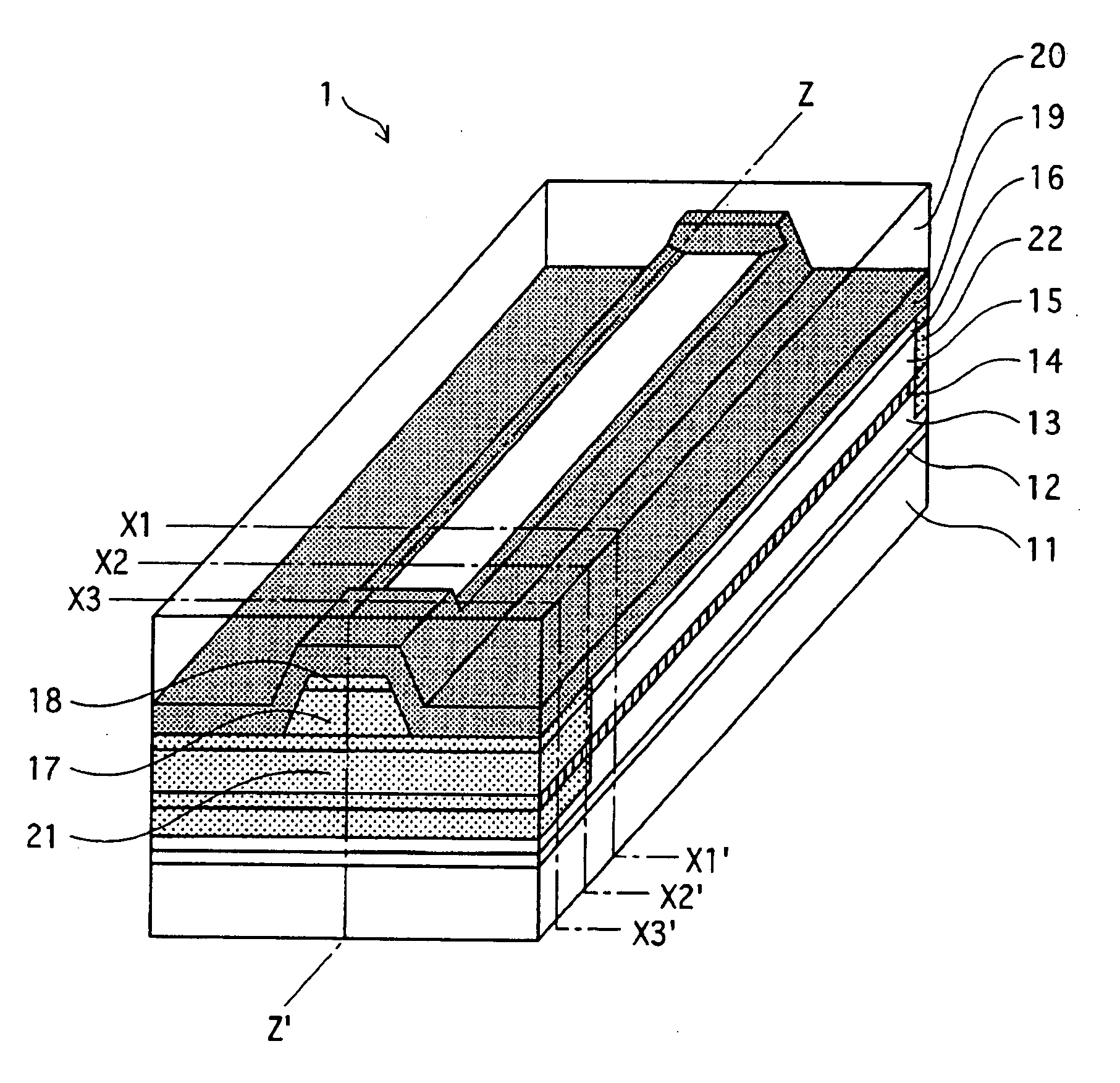
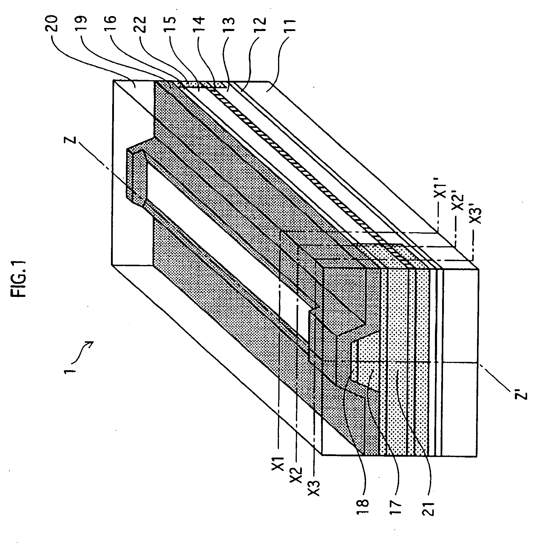
[0057]FIG. 1 is a perspective view showing a semiconductor laser device 1 according to the embodiment of the present invention.

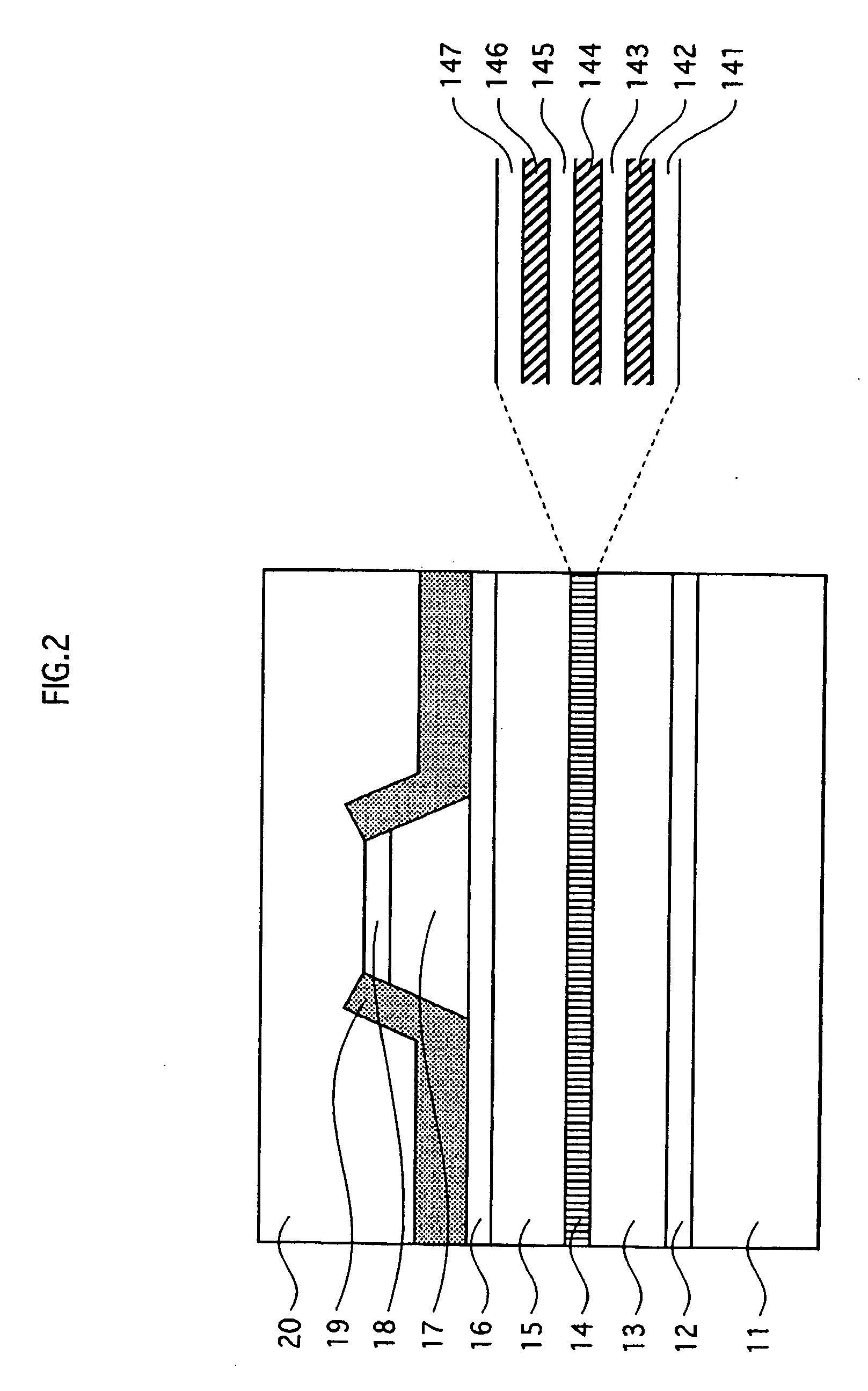
[0058] The semiconductor laser device 1 is formed by laminating an n-type semiconductor substrate 11, an n-type buffer layer 12, an n-type cladding layer 13, a quantum well active layer 14, a p-type first cladding layer 15, an etching stop layer 16, a p-type second cladding layer 17, a p-type cap layer 18, a current blocking layer 19, and a p-type contact layer 20, in this order. In the drawing, the p-type contact layer 20 is shown transparent for better viewing.

[0059] The n-type cladding layer 13 to the p-type second cladding layer 17 constitute an optical waveguide. A light emitting end face (the front face in FIG. 1) and an opposite end face of the optical waveguide are coated with a reflection film (not illus...


PUM


Abstract

To provide a semiconductor laser device for which a horizontal divergence angle of a laser beam can be improved independently of optimization of other properties such as a cladding layer thickness and a current injected region size. A current blocking layer covers a larger area of a p-type second cladding layer and p-type cap layer extending in a resonator length direction, on a light emitting end face side than on an opposite end face side. Thus, current uninjected regions are formed in an optical waveguide. The current blocking layer (current uninjected region) on the light emitting end face side is set long enough to prevent carriers, which flow in from a current injected region, from reaching alight emitting end face. In this way, a light intensity distribution of a near-field pattern on the light emitting end face is concentrated, thereby increasing a horizontal divergence angle of a laser beam.

Description

[0001] This application is based on an application No. 2003-272287 filed in Japan, the contents of which are hereby incorporated by reference. BACKGROUND OF THE INVENTION [0002] 1. Field of the Invention [0003] The present invention relates to a semiconductor laser device, and in particular relates to techniques for independently controlling increases in light output power and increases in horizontal divergence angle. [0004] 2. Related Art [0005] Optical discs such as CD (Compact Disc) and DVD (Digital Versatile Disc) are widely used in recent years. Nowadays, optical discs gain widespread acceptance among consumers as media suitable for recording large-volume digital information represented by AV (Audio / Video) content information. As a result, demand for optical disc devices capable of writing onto optical discs is growing sharply. [0006] A writing speed of an optical disc device can be improved by increasing light output power of a semiconductor laser device which is used in an op...

Claims


Application Information

Patent Timeline
IPC IPC(8): H01S5/00H01S5/227H01S5/16H01S5/22H01S5/223H01S5/30H01S5/323H01S5/343H01S5/40
CPCB82Y20/00H01S5/162H01S5/168H01S5/221H01S5/2231H01S5/305H01S5/3054H01S5/32341H01S5/34326H01S5/3436H01S5/4031H01S5/4087H01S2301/185
Inventor UEDA, TETSUOKUME, MASAHIROKAWATA, TOSHIYAKIDOGUCHI, ISAO
Owner PANASONIC CORP
Learn More