
Eureka
For R&D, Eureka makes reading and utilizing patents & technical documents easy.
Eureka AIR
Designed for self-driven R&D workflows. Generate viable solutions, solve complex R&D challenges, empower your innovation with AI.

Eureka Materials
Designed for material experts only. Revolutionize your material R&D, from search, analyze, to developing new materials.

TechResearch
Generate reliable direction feasibility study reports for your R&D in just a few steps.

TechSeek
Discover and master advanced knowledge NOW. Basics, ideas, possibilities, all at once.

TechMind
As an expert in R&D Theories, TechMind can generates customized viable solutions instantly.

TechRisk
Analyze your overall solution with one click, know your potential R&D risks in advance.

TechMonitor
Get weekly tech updates, stay abreast of the latest tech innovations and key insights.
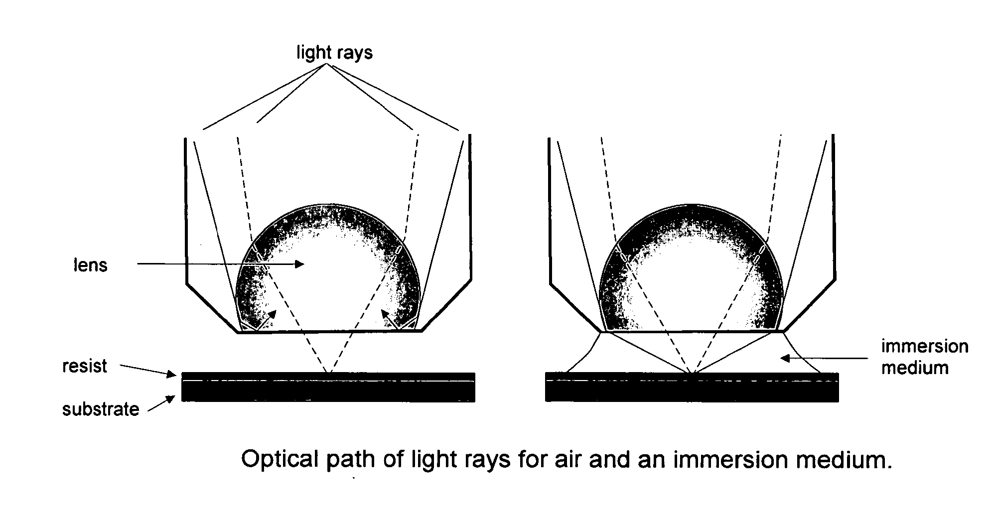
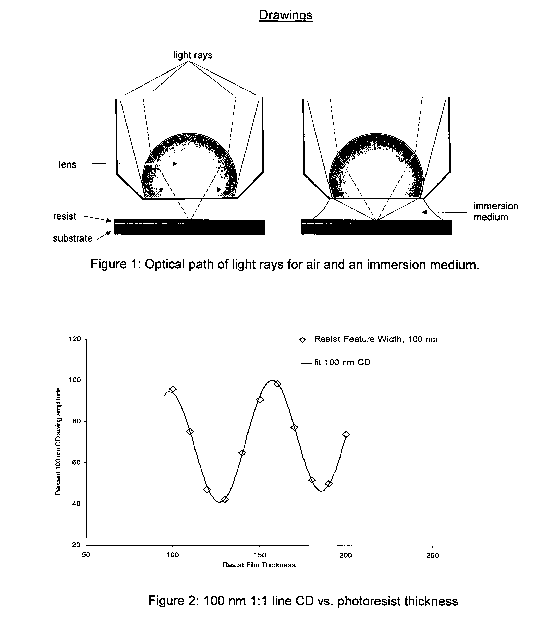
Process of imaging a photoresist with multiple antireflective coatings
- Summary
- Abstract
- Description
- Claims
- Application Information
AI Technical Summary
Problems solved by technology
Method used
Image

Examples
example 1
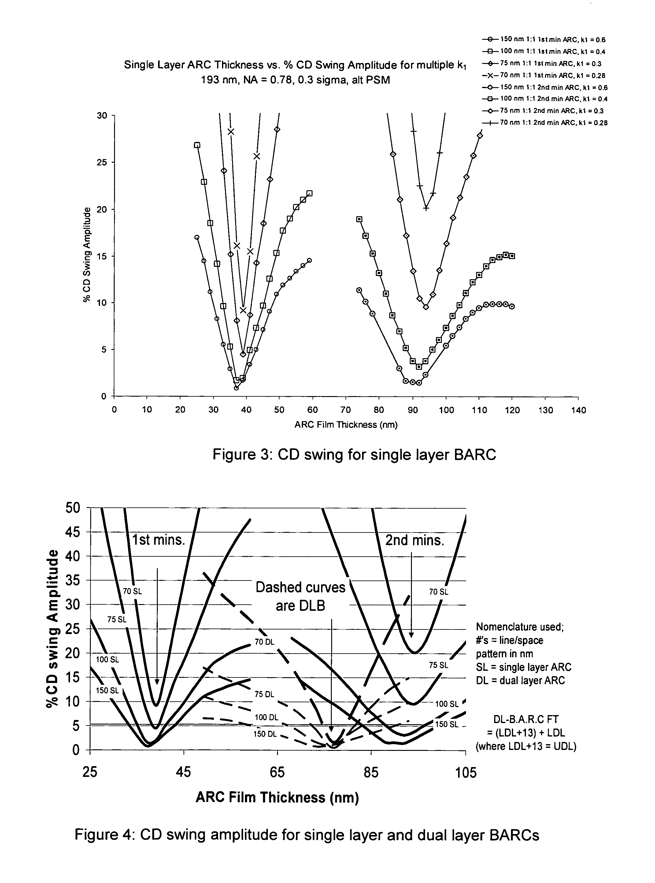
[0054] Computer simulation studies were carried out in Prolith v8. 1 (available from Finle Corp. Austin, Tex.) to investigate the comparative performance of three organic antireflective systems: two single-layer BARCs designed for 1st and 2nd minimum film thickness application, and the dual layer BARC system.
[0055] The response evaluated was substrate reflectivity, Sr, and the % resist critical dimension (CD) swing amplitude evaluated for a range of k1 values ranging from 0.6 to 0.28 at 193 nm. The inputs for all BARCs were film thickness. The optical constants for each BARC were fixed; the film thickness (FT) ranges evaluated were for:
Single Layer BARC:
For 1st min SLR: AZ® 1C5D, FT 20 nm to 80 nm, n=1.6−0.51i at 193 nm
For 2nd min SLR: AZ® ArF38, FT 50 nm to 120 nm, n=1.7−0.34 i at 193 nm
Dual layer: Upper Layer BARC, FT 13 nm to 77 nm, n=1.702−0.196i at 193 nm; Lower Layer BARC, 0 nm to 64 nm, n=1.904−0.67i at 193 nm
[0056] The AZ® solutions are available from AZ® Electroni...
example 2
Synthesis of Polymer for Lower Layer Antireflective Coating (LDL1)
[0063] 83.2 g of benzyl methacrylate, 25.8 g of hydroxyethyl methacrylate, 500 ml tetrahydrofuran (THF) and 2 g 2,2 azobisisobutyronitrile (AIBN) were combined, in that order, to a 1 L round bottom flask. The solution was refluxed for 12 hr under nitrogen. After cooling, the polymer was recovered by precipitation into 4 L of hexane, filtered and dried in a vacuum desiccator. The polymer was produced with a 98.5% yield. The reaction scheme for this procedure is shown below. The molecular weight of the HB polymer as measured using GPC with a polystyrene standard was 30,000. The NMR for the polymer was measured using 300 MHZ, H1-spectrum in acetone-d6, and the results were S, br, 7.35 ppm, 5H, phenyl protons; S, br, 7.35 ppm, 2H, CH2-phenyl; M, br, 3.6 to4.2 ppm, 1H O—CH2—CH2.
example 3
Formulation of Lower Layer Antireflective Coating
[0064] The formulation consisted of 9.21 g of HB copolymer (Example 2), 2.76 g MX-270 (available from Sanwa Chemical Co Ltd. 6520, Tamura, Hiratuka-city, Kanagawa, Japan), 2 g dodecylbenzylsulfonium triethylammonium salt, 2 g of p-toluenesulfonic acid triethylammonium salt, and 460 g 70 / 30 PGMEA / PGME.
PUM
 Abstract
Description
Claims
Application Information
 - R&D Engineer
- R&D Manager
- IP Professional
- Industry Leading Data Capabilities
- Powerful AI technology
- Patent DNA Extraction
Browse by: Latest US Patents, China's latest patents, Technical Efficacy Thesaurus, Application Domain, Technology Topic, Popular Technical Reports.
© 2024 PatSnap. All rights reserved.Legal|Privacy policy|Modern Slavery Act Transparency Statement|Sitemap|About US| Contact US: help@patsnap.com