Multilayer substrate and method for producing same

a multi-layer substrate and substrate technology, applied in the field of multi-layer substrates and electronic components, can solve the problems of insufficient original electrical characteristic of materials, poor crystallinity of ceramic dielectric films formed by thin film methods, and difficult to fetch capacitor elements having high capacity into substrates with conventional substrate structures, etc., to achieve excellent electrical characteristics, high reliability, and high density

Inactive Publication Date: 2006-08-17
TDK CORPARATION
View PDF19 Cites 37 Cited by
  • Summary
  • Abstract
  • Description
  • Claims
  • Application Information

AI Technical Summary

Benefits of technology

[0009] Therefore, it is an object of the invention to obtain an organic multilayered substrate which can include a functional element having an excellent electrical characteristic at a high density and has a high reliability, and a manufacturing method thereof.

Problems solved by technology

For example, it is hard to fetch a capacitor element having a high capacity into a substrate with a conventional substrate structure.
Moreover, there is a problem in that a ceramic dielectric film formed by a thin film method generally has a poor crystallinity and the original electrical characteristic of a material cannot be exhibited sufficiently.
However, an ordinary resin substrate has a heating limit of approximately 200° C. and heating is limited to at most approximately 400° C. even if polyimide having a high heat resistance is used.
In the case in which the surface of the organic resin substrate is generally provided with a concavo-convex portion in order of several μm and has a poor smoothing property and a thin film having a thickness of approximately several tens nm is formed on the surface (a concavo-convex portion which is several hundred times as great as the thickness of a film is present on the surface of the resin substrate), furthermore, there is also a problem in that a defect is easily generated.
For this reason, a manufacturing process becomes complicated, and furthermore, an adhesive layer is to be always provided between the material regions.
In respect of a mounting density, therefore, a sufficient structure has not been obtained yet.
Moreover, there is also caused a problem in that a crack or breakage 96 is easily generated between both of the material films due to a difference between the thermal shrinkage ratios of the both of the materials 91 and 92.
On the other hand, in some cases in which both of the functional material films are to formed by an organic material (a resin), the bonding strength of the contact portion of both of the material films is small and a clearance is generated between both of the films to deteriorate the reliability of the substrate.

Method used


Image

  • Multilayer substrate and method for producing same
  • Multilayer substrate and method for producing same
  • Multilayer substrate and method for producing same

Examples


first embodiment

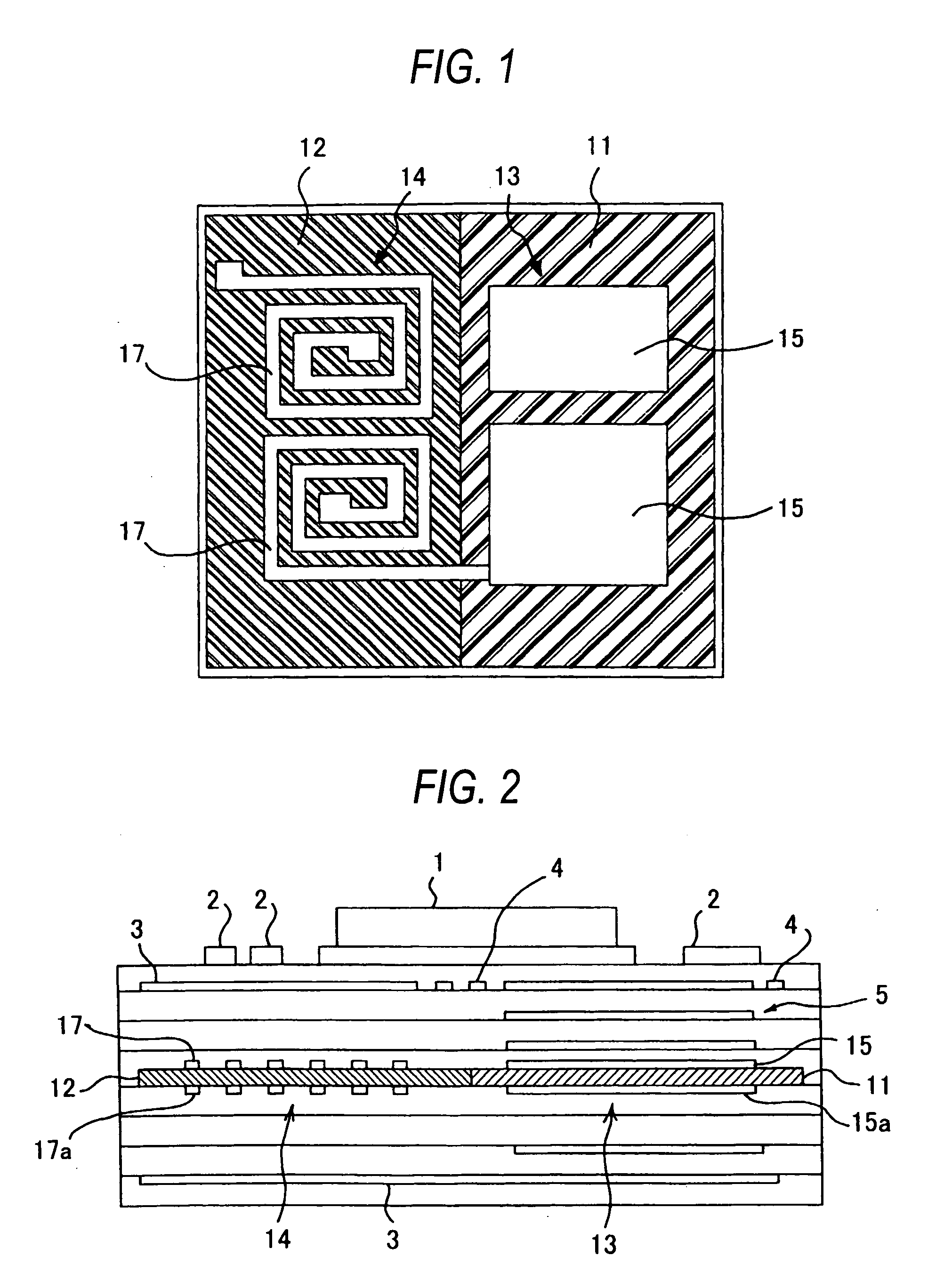
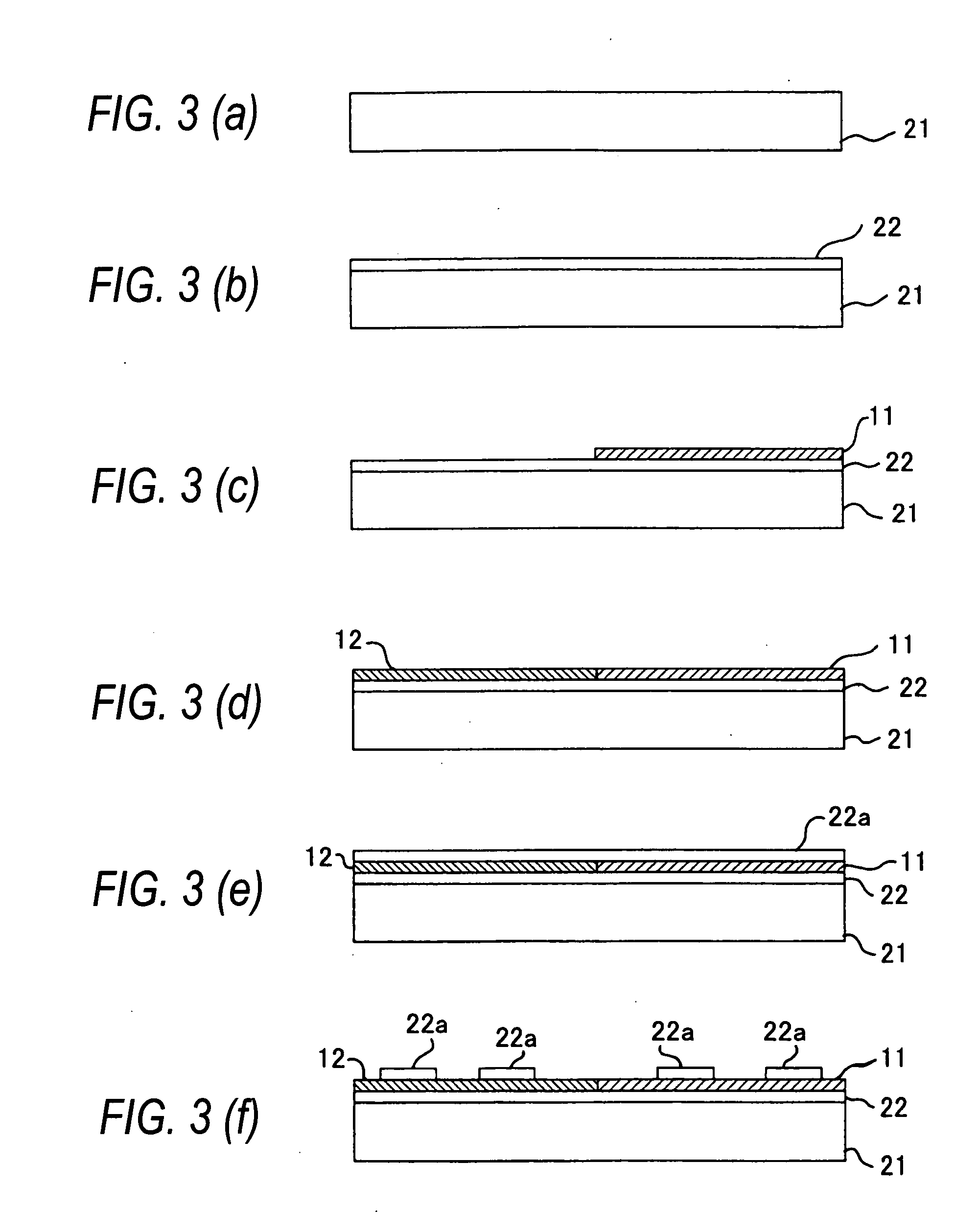
[0042]FIGS. 1 and 2 show a multilayered substrate according to an embodiment of the invention. As shown in FIGS. 1 and 2, the multilayered substrate has such a structure that thin films 11 and 12 formed by different materials are provided in the same plane on the inside of the substrate, and different kinds of functional elements, a capacitor 13 having a high capacity and an inductor 14 are provided on the same layer in the substrate by the thin films.

[0043] More specifically, in the embodiment, the high dielectric material thin film 11 is formed as a first functional material film by a material having a high dielectric constant and the low dielectric material thin film 12 is formed as a second functional material film by a material having a low dielectric constant. Electric conductors 15 and 15a patterned rectangularly are provided on both surfaces of the high dielectric material thin film 11 to form the capacitor 13 having a high capacity (the first functional element), while ele...

second embodiment

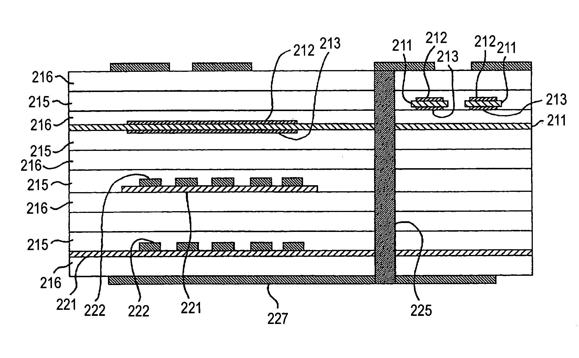
[0069]FIGS. 4 and 5 show a multilayered substrate according to a second embodiment of the invention. As shown in these drawings, the multilayered substrate have four layers in which a core substrate 31 including different kinds of material films 11 and 12 on one surface and an electric conductor pattern32 for bare chip mounting on the other surface and the other substrate 35 including a wiring pattern 36 on one surface and a ground pattern 37 and a land pattern 38 on the other surface are integrated with a prepreg 39 interposed therebetween, and a bare chip 7 can be flip chip mounted on the surface of the substrate.

[0070] The core substrate 31 having different kinds of material films has the high dielectric material thin film 11 (the first functional material film) and the low dielectric material thin film 12 (the second functional material film) formed on one of surfaces (a lower surface) thereof, and a capacitor 13 having a high capacity is formed in a high dielectric material th...

third embodiment

[0086]FIGS. 7 and 8 show a multilayered substrate according to a third embodiment of the invention. While two different kinds of material films (the high dielectric material thin film and the low dielectric material thin film) are provided in the same layer in the substrate in the first and second embodiments, a thin film constituted by a magnetic material, a magnetic thin film 61 (a third functional material film), a thin film constituted by a ceramic semiconductor material, and a semiconductor thin film 62 (a fourth functional material film) are provided and four kinds of functional material films in total are formed on the same layer surface in addition to a high dielectric material thin film 11 (a first functional material film) and a low dielectric material thin film 12 (a second functional material film) as shown in FIG. 7 in the substrate according to the embodiment.

[0087] Then, an electric conductor 15 patterned rectangularly and an electric conductor 17 patterned spirally ...


PUM

PropertyMeasurementUnit
thicknessaaaaaaaaaa
temperatureaaaaaaaaaa
heat resistanceaaaaaaaaaa

Abstract

In a multilayered substrate obtained by laminating a plurality of substrates and including plural kinds of functional elements therein, a first functional material film and a second functional material film are provided on the same plane and first and second functional elements are formed by the first and second functional material films, respectively. The functional material film may be formed on a transferring substrate by a thin film method and may be transferred to the substrate.

Description

TECHNICAL FIELD [0001] The present invention relates to a multilayered substrate and an electronic component using the same, and a method of manufacturing them, and more particularly to the structure and manufacturing method of a multilayered substrate provided with a functional element such as a capacitor or an inductor in an organic resin substrate. BACKGROUND ART [0002] With the development of a reduction in the size and thickness of an electronic apparatus such as a cell phone or a notebook computer, and an increase in a function and an enhancement in a performance, recently, a reduction in a size and thickness and an enhancement in a performance of a substrate to be used for them have been demanded greatly. For this reason, there has been proposed various substrate structures in which the substrate can be multilayered and a functional element such as a capacitor, an inductor or a resistor can be provided therein to carry out high density mounting. [0003] An organic multilayered...

Claims


Application Information

Patent Timeline
Patent Type & Authority Applications(United States)
IPC IPC(8): H05K1/09H05K1/16H05K3/46
CPCH01L23/642Y10T29/49126H05K1/162H05K1/165H05K3/4611H05K3/4652H05K2201/0187H05K2201/09672H05K2203/0537H01L2924/19015H01L2924/15311H01L2224/73204H01L2224/32225H01L2224/16225H01L2924/00H01L2224/05573H01L2224/05568H01L2924/00014H01L2224/05599H05K3/46
Inventor TAKAYA, MINORUENDO, TOSHIKAZUKOBUKE, HISASHISASAKI, MASAMIKAJINO, TAKASHIGOTO, KATSUYOSHI
Owner TDK CORPARATION
Why Eureka
Try Eureka