Memory element and memory device

a memory element and memory technology, applied in the field of memory elements, can solve the problems of heat damage to the mos transistor formed in advance, difficult mass production at low cost, and inability to meet the requirements of production, etc., and achieve the effects of reducing production costs, reducing production costs, and ensuring the effect of quality

Active Publication Date: 2006-08-24
SONY SEMICON SOLUTIONS CORP
View PDF8 Cites 19 Cited by
  • Summary
  • Abstract
  • Description
  • Claims
  • Application Information

AI Technical Summary

Benefits of technology

[0045] Further, since data is recorded by means of the change in the resistance value, data can be recorded and the recorded data can be retained easily even if the memory element is made miniaturized.
[0046] Hence, according to the present invention, a memory device in which data can stably be recorded and erased and which can easily be manufactured with a comparatively simplified method is obtained.

Problems solved by technology

However, in the above-described memory element having the structure in which Cu, Ag, Zn are contained either in the upper electrode or in the lower electrode and a Ges or GeSe amorphous chalcogenide material is positioned between the electrodes, such problems as the crystallization of a chalcogenide thin film due to temperature rise, the change in properties of materials due to the crystallization, and data originally retained in a high resistance state being made into the data in a low resistance state under the high temperature environment or after a long-time storage.
Further, in the case in which a crystalline material is used as a recording material between the upper and lower electrodes, problems tend to occur compared with the case in which an amorphous material is used, and therefore mass production at low costs has been difficult.
Further, in order to obtain a high-quality crystallinity, high temperature treatment of 700° C., for example, is needed and there may be a problem that properties of a MOS transistor formed in advance may deteriorate due to heat.
Furthermore, in order to obtain crystal growth, base materials therefor are limited and a single-crystal material is required, for example.

Method used


Image

  • Memory element and memory device
  • Memory element and memory device
  • Memory element and memory device

Examples


experiment 1

[Experiment 1]

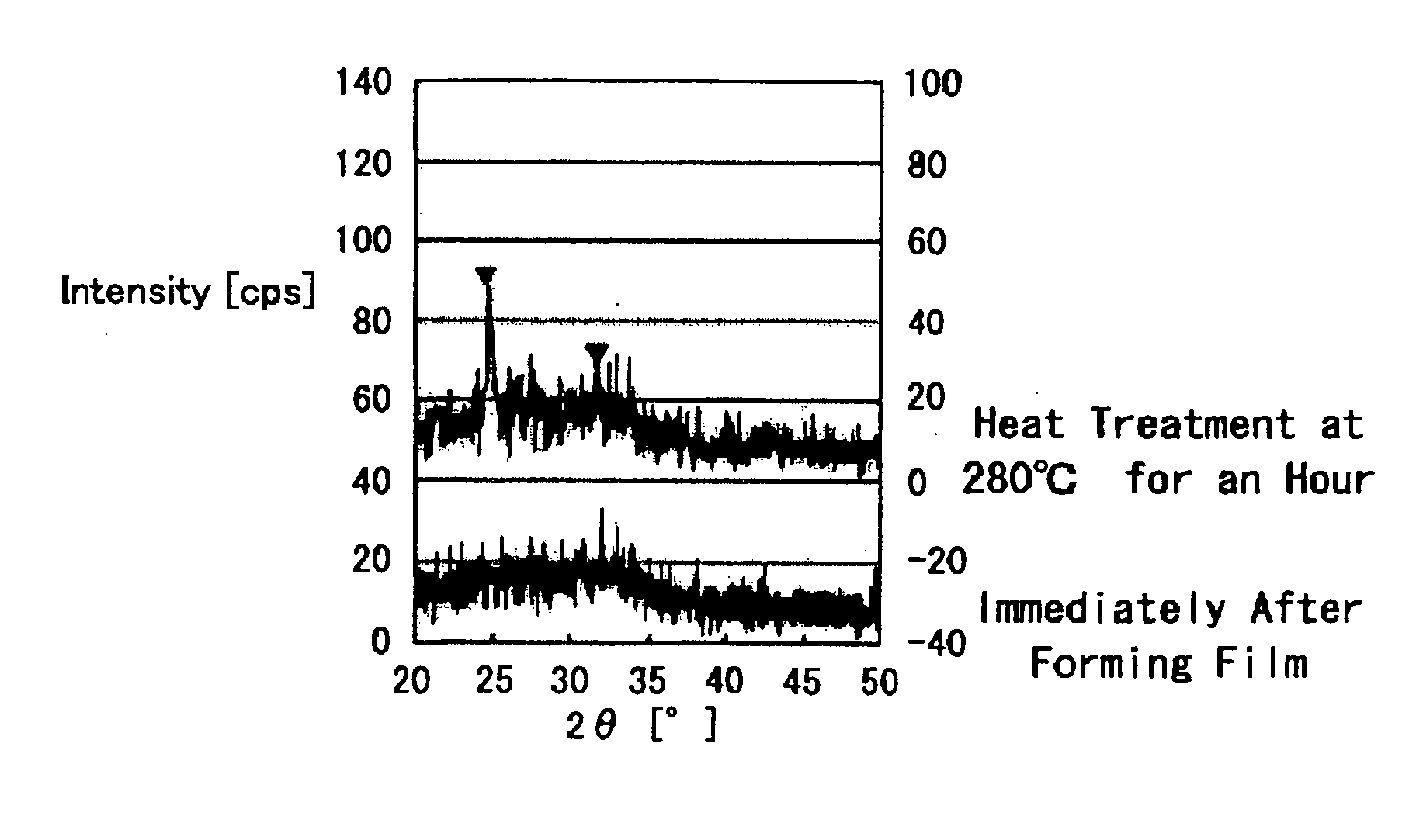
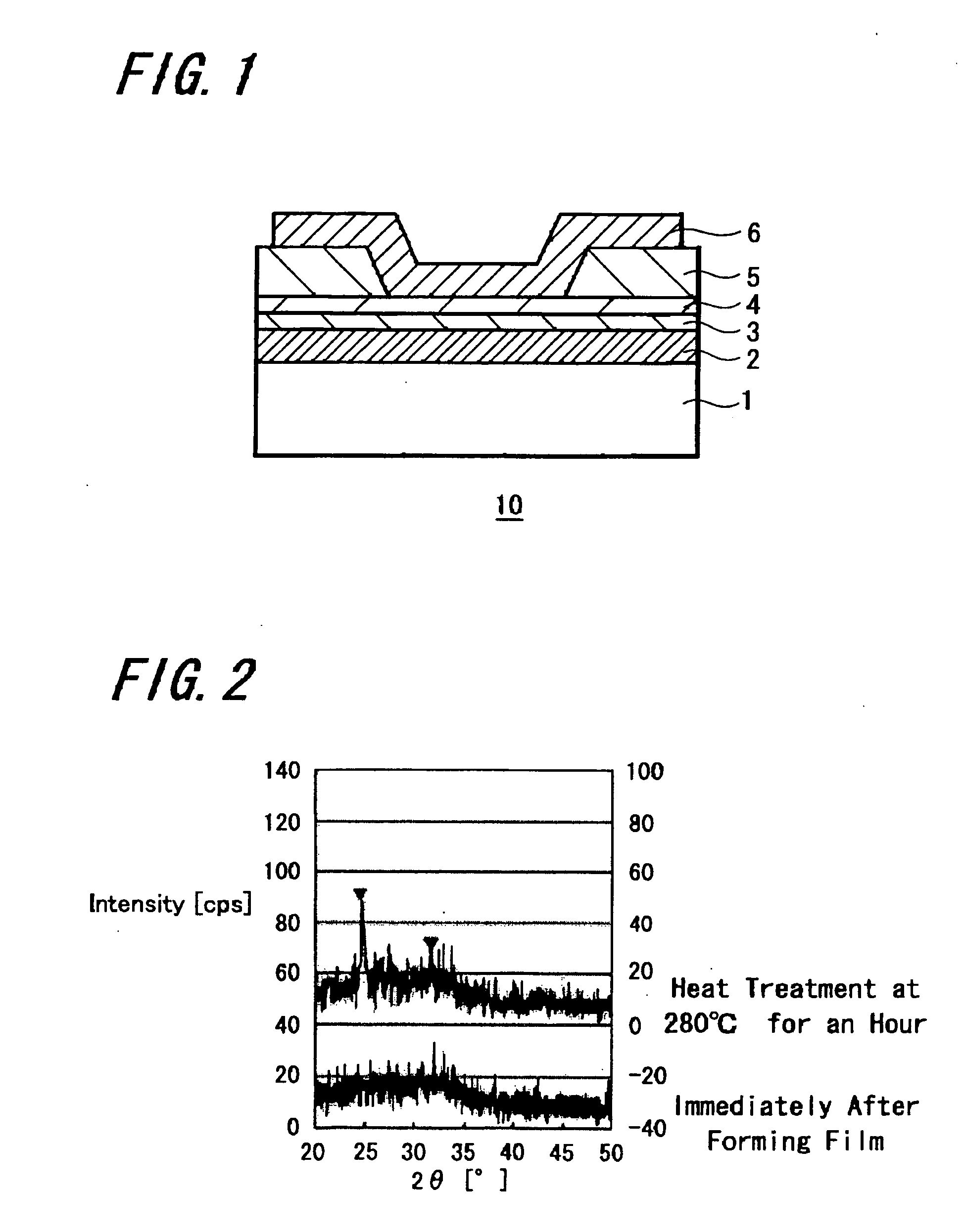
[0153] On a silicon substrate, a WN film of 20 nm in thickness was deposited as the lower electrode 2, a Cu61Te21Ge5B8 film was formed thereon as the ion source layer 3, an GdN film of 2.5 nm in thickness was formed as the memory thin film 4 and photoresist was formed to cover the surface, and after that, exposure and development were performed by means of photolithography to form an opening (through hole) in the photoresist on the memory thin film 4.

[0154] After that, air was evacuated to be a vacuum and then replaced with nitrogen atmosphere to perform annealing treatment in the nitrogen atmosphere and the photoresist was transformed to be the insulation layer 5 as hard-cured resist which is stable with respect to temperature, etching and the like. It should be noted that hard-cured resist was used as the insulation layer 5 because of convenience to be formed in simple and easy manner in the experiment, and when manufacturing commercial products, it is preferable th...

experiment 2

[Experiment 2]

[0168] A Cu61Te27Ge7Gd5 film was formed as the ion source layer 3, and a memory element 10 of a sample 11 was obtained in which the other structure was similar to the sample 9.

[0169] Further, a Cu56Te25Ge6Gd5B8 film was formed as the ion source layer 3, and a memory element 10 of a sample 12 was obtained in which the other structure was similar to the sample 9.

[0170] Further, a Cu51Te23Ge6Gd5B15 film was formed as the ion source layer 3, and a memory element 10 of a sample 13 was obtained in which the other structure was similar to the sample 9.

[0171] Further, a Cu49Te21Ge5Gd4B20 film was formed as the ion source layer 3, and a memory element 10 of a sample 14 was obtained in which the other structure was similar to the sample 9.

[0172] Among those samples, each of the samples 12 to 14 has a structure according to a practice example of the memory element of the present invention, and the sample 11 has a structure of a comparative example.

[0173] After the heat treat...

experiment 3

[Experiment 3]

[0177] A memory element in which the ion source layer 3 contains rare-earth elements and silicon (Si) was made and the I-V characteristic was studied.

[0178] A Cu51Te31Ge8Gd6Si4 film was formed as the ion source layer 3, and a memory element 10 of a sample 15 was obtained in which the other structure was similar to the sample 9.

[0179] Further, a Cu48Te28Ge7Gd6Si12 film was formed as the ion source layer 3, and a memory element 10 of a sample 16 was obtained in which the other structure was similar to the sample 9.

[0180] Further, a Cu40Te24Ge6Gd5Si26 film was formed as the ion source layer 3, and a memory element 10 of a sample 17 was obtained in which the other structure was similar to the sample 9.

[0181] After the heat treatment in nitrogen atmosphere at 280° C. was performed on each memory element of those samples 15 to 17, I-V characteristic was measured. Measurement results of the I-V characteristic were shown in FIG. 11A to 11C. FIG. 11A shows measurement resul...


PUM


Abstract

A memory element in which data recording and data readout can be performed stably without difficulties and which can be manufactured with a comparatively simplified method is provided.
The memory element 10 includes a memory layer 4 and an ion source layer 3 positioned between the first electrode 2 and the second electrode 6, in which the ion source layer 3 contains any of elements selected from Cu, Ag, Zn and any of elements selected from Te, S, Se, and the ion source layer further contains boron (or rare-earth elements and silicon).

Description

CROSS REFERENCES TO RELATED APPLICATIONS [0001] The present invention contains subject matter related to Japanese Patent Application JP 2005-004178 filed in the Japanese Patent Office on Jan. 11, 2005, the entire contents of which being incorporated herein by reference. BACKGROUND OF THE INVENTION [0002] 1. Field of the Invention [0003] The present invention relates to a memory element in which data can be recorded and a memory device including the memory element. [0004] 2. Description of the Related Art [0005] In information devices such as a computer, a DRAM capable of high speed operation and having high density is widely used as a random access memory. [0006] However, since the DRAM has a complicated manufacturing process compared with a typical logic circuit LSI and signal processing employed in an electronic apparatus, manufacture costs increase. [0007] Further, since the DRAM is a volatile memory in which data disappears when the power is shut off, such refreshing operation t...

Claims


Application Information

Patent Timeline
Patent Type & Authority Applications(United States)
IPC IPC(8): H01L21/8236H01L29/76
CPCH01L27/101H01L27/115H01L45/145H01L45/085H01L45/1233H01L45/1266H01L45/146H01L45/1625H10N70/245H10N70/8416H10N70/883H10N70/026H10N70/8833H10N70/826H10B69/00B26D7/0625B26D7/0633A23L17/60B26D2210/02
Inventor MIZUGUCHI, TETSUYAARATANI, KATSUHISAMAESAKA, AKIHIROKOUCHIYAMA, AKIRA
Owner SONY SEMICON SOLUTIONS CORP
Why Eureka
Try Eureka