Fabrication method of a low-temperature polysilicon thin film transistor

a technology of polysilicon thin film and fabrication method, which is applied in the direction of transistors, semiconductor devices, electrical equipment, etc., can solve the problems of device degradation, complex ldd process, and limited choice of substrate materials to apply to the process, so as to improve device performance

Active Publication Date: 2006-09-07
SCHLUMBERGER TECH CORP
View PDF10 Cites 12 Cited by
  • Summary
  • Abstract
  • Description
  • Claims
  • Application Information

AI Technical Summary

Benefits of technology

[0012] Accordingly, the present invention is directed to a fabrication method of a low-temperature polysilicon thin film transistor (LTPS-TFT) to improve device performance by forming an amorphous silicon hot carrier restrain region.
[0013] The present invention is also directed to a method of fabricating a LTPS-TFT. The method is capable of reducing manufacturing costs as well as improving device performance by forming an amorphous silicon hot carrier restrain region.
[0014] The present invention discloses a LTPS-TFT. The LTPS-TFT comprises a gate, a dielectric gate, a patterned silicon layer, a patterned insulating layer, an ohmic contact layer, and a source / drain layer which are sequentially formed on a substrate. The patterned silicon layer is disposed on the gate dielectric layer and directly over the gate. The patterned silicon layer comprises a polysilicon channel region and an amorphous silicon hot carrier restrain region adjacent thereto. Also, the patterned silicon layer further comprises an edge portion (i.e. a portion of the patterned silicon layer other than the polysilicon channel region and the hot carrier restrain region) underneath the ohmic contact layer. The amorphous silicon hot carrier restrain region is capable of reducing hot carrier effect, preventing degradation of the transistor during the operation of the transistor. The patterned insulating layer covers the patterned silicon layer. The ohmic contact layer is disposed on the edge portion of the patterned silicon layer and a portion of the insulating layer over the amorphous silicon hot carrier restrain region to expose a portion of the patterned insulating layer and contacting the amorphous silicon hot carrier restrain region. The source / drain layer is disposed on the ohmic contact layer, or even on a portion of the substrate.
[0025] Compared with the prior art method of fabricating LTPS-TFT, the fabrication method of the present invention saves a lightly-doped drain (LDD) process and a LDD mask. The manufacturing cost, therefore, is reduced. Moreover, the LTPS-TFT of the present invention has the advantages of high driving current of polysilicon thin film transistors and low leakage current of amorphous thin film transistors.

Problems solved by technology

The prior art method of fabricating the polysilicon TFT requires a high temperature process up to 1000° C. Due to the high temperature requirement, the choice of the substrate material that can be applied to the process is limited.
The polysilicon TFT is easy to induce hot carrier effect at the drain region, causing device degradation.
In addition, the LDD process is so complicated that the method of fabricating the prior art LTPS-TFT has high manufacturing cost.

Method used


Image

  • Fabrication method of a low-temperature polysilicon thin film transistor
  • Fabrication method of a low-temperature polysilicon thin film transistor
  • Fabrication method of a low-temperature polysilicon thin film transistor

Examples


first embodiment

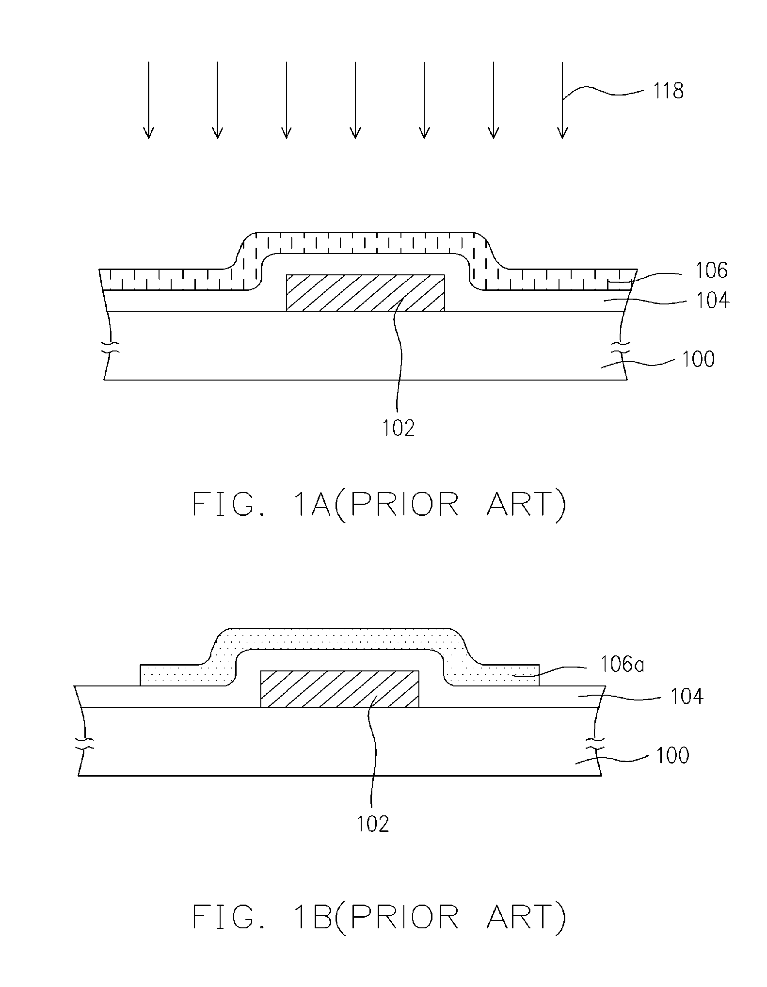
[0033]FIGS. 2A-2H are cross-sectional views showing progression steps of the method of fabricating a LTPS-TFT according to the present invention. Referring to FIG. 2A, a gate 202, a gate dielectric layer 204, a first amorphous silicon layer 206 and a patterned insulating layer 208 are sequentially formed on a substrate 200. The patterned insulating layer 208 is formed on the first amorphous silicon layer 206, and over the gate 202. In this embodiment, the material of the patterned insulating layer 208 includes, for example, silicon nitride, silicon oxide or other dielectric materials.

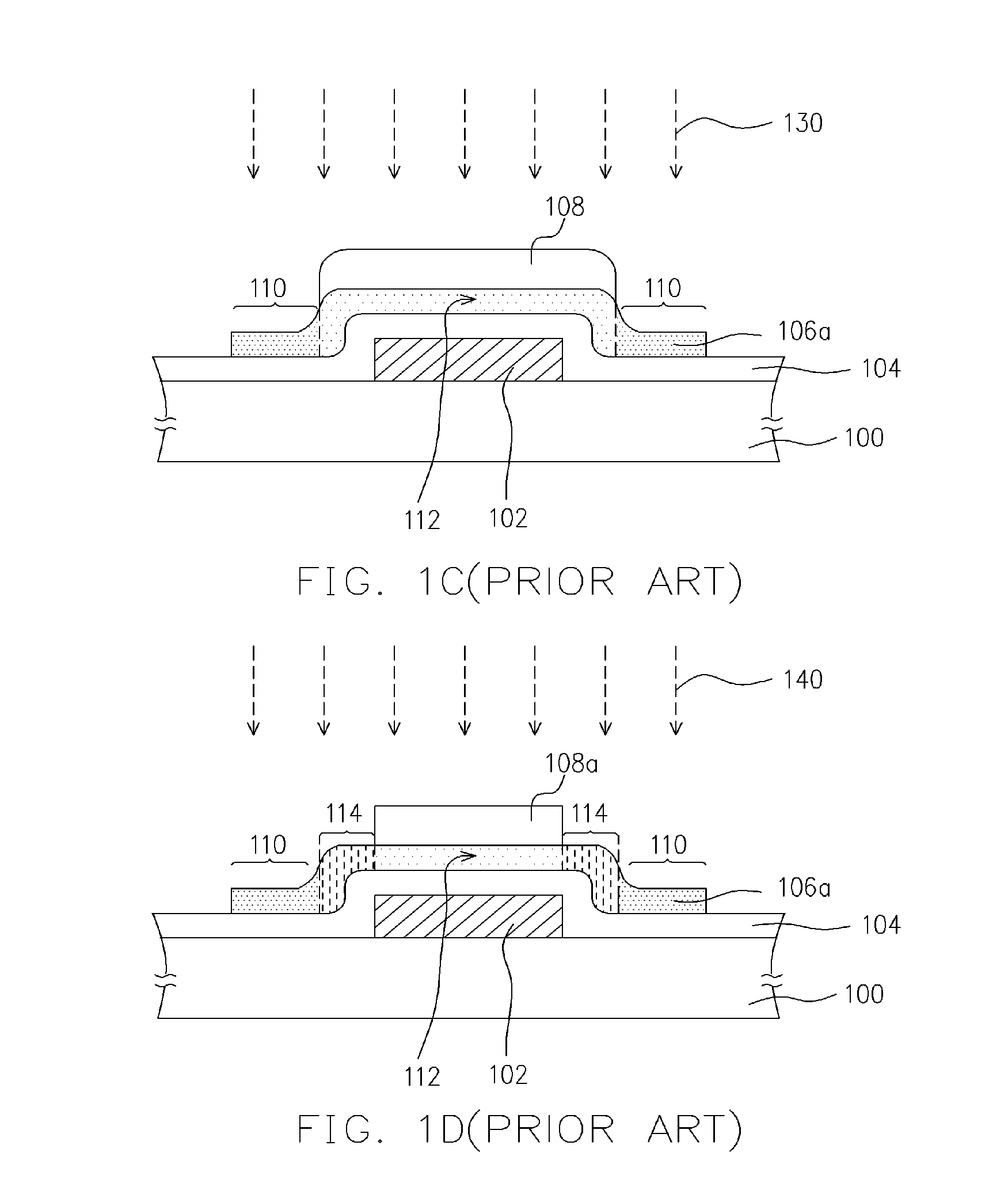
[0034] Referring to FIG. 2B, the patterned insulating layer 208 serves as a mask for an implantation process, such as ion implantation. The doping ions 230 is doped into a portion of the first amorphous silicon layer 206, which is not covered by the patterned insulating layer 208 to reduce the resistance thereof. It serves as the ohmic contact layer in the subsequent process. The doping ions 230 can be ...

second embodiment

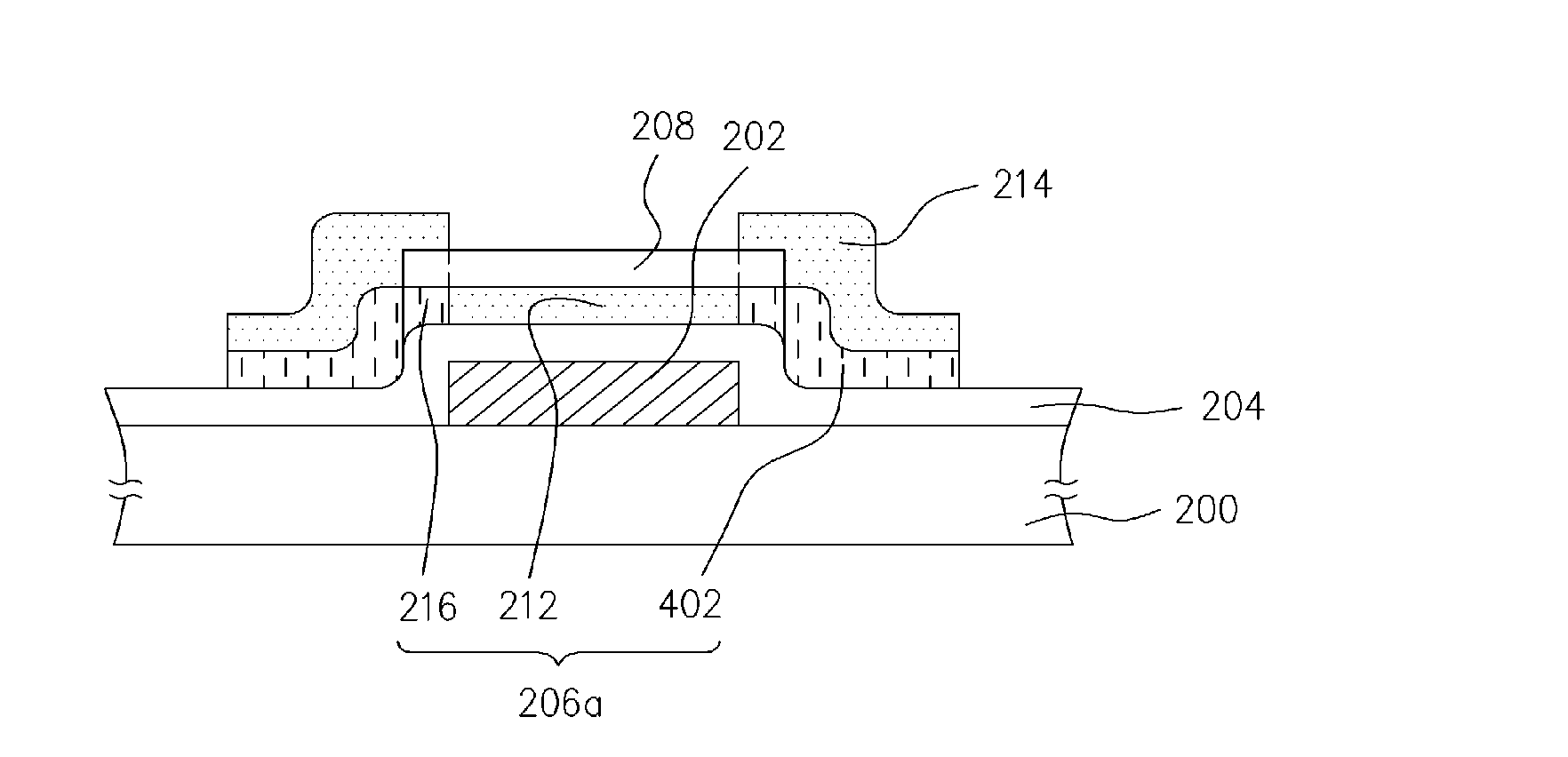
[0043]FIGS. 3A-3C are cross-sectional views showing partial steps of the method of fabricating a LTPS-TFT according to the present invention. Referring to FIG. 3A, after forming the first patterned amorphous silicon layer 206a and the second patterned amorphous silicon layer 210a according to the processes of FIGS. 2A-2D, the source / drain layer 218 is formed on the second patterned amorphous silicon layer 210a and the gate dielectric layer 204. The second patterned amorphous silicon layer 210a serves as the ohmic contact layer of the thin film transistor.

[0044] Referring to FIG. 3B, the structure formed in FIG. 3A is exposed to the excimer laser beams 222. During the annealing process, the first patterned amorphous silicon layer 206a above the gate 202 is melted and then recrystalized, transforming into the polysilicon channel region 212 as shown in FIG. 3C. Because of the excellent thermal conductivity of the source / drain layer 218, the second patterned amorphous silicon layer 210a...

third embodiment

[0046]FIGS. 4A-4B are cross-sectional views showing partial steps of the method of fabricating a LTPS-TFT according to the present invention. Referring to FIG. 4A, after forming the patterned insulating layer 208 over the substrate 200 in accordance with FIG. 2A, a second amorphous silicon layer 310 is formed on the first amorphous silicon layer 206 to cover the patterned insulating layer 208. The second amorphous silicon layer 310 can be, for example, a doped or an undoped amorphous silicon layer.

[0047] Referring to FIG. 4B, a first patterned amorphous silicon layer 206a and a second patterned amorphous silicon layer 310a are formed according to the description of FIG. 2D. The patterned insulating layer 208 serves as a mask for an implantation process to implant ions 230 into the first patterned amorphous silicon layer 206a and the second patterned amorphous silicon layer 310a. The subsequent processes are similar to those of the last embodiments.

[0048] In the fourth embodiment, a...


PUM


Abstract

An LTPS-TFT structure comprises a gate, a gate dielectric layer, a patterned silicon layer, a patterned insulating layer, an ohmic contact layer and a source / drain layer. The gate and the gate dielectric layer are disposed on the substrate. The patterned silicon layer and the patterned insulating layer are disposed on the gate dielectric layer over the gate. The patterned silicon layer comprises a polysilicon channel region and an amorphous silicon hot carrier restrain region. The ohmic contact layer is disposed on a portion of the patterned silicon layer other than the polysilicon channel region and the amorphous silicon hot carrier restrain region and a portion of the patterned insulating layer over the amorphous silicon hot carrier restrain region. The source / drain layer is disposed on the ohmic contact layer and the gate dielectric layer.

Description

CROSS-REFERENCE TO RELATED APPLICATION [0001] This application is a divisional of a prior application Ser. No. 10 / 710,844, filed Aug. 6, 2004, which claims the priority benefit of Taiwan application serial no. 93109432, filed Apr. 6, 2004. All disclosures are incorporated herewith by reference. BACKGROUND OF THE INVENTION [0002] 1. Field of the Invention [0003] The present invention relates to a fabrication method of a transistor, and more particularly to a fabrication method of a low-temperature polysilicon thin film transistor (LTPS-TFT). [0004] 2. Description of the Related Art [0005] Generally, devices use switches to control the operation thereof. For example, active matrix displays use thin film transistors (TFT) as driving components. According to the material of a channel layer of the TFT, the types of the TFT include amorphous silicon TFT and polysilicon TFT. Based on the position of the channel layer corresponding to that of the gate, the types of TFT also include top-gate...

Claims


Application Information

Patent Timeline
Patent Type & Authority Applications(United States)
IPC IPC(8): H01L21/84H01L21/20H01L21/00H01L21/265H01L21/336H01L29/786H01L31/036
CPCH01L29/66765H01L29/78678H01L29/78621
Inventor KUO, CHENG-CHANG
Owner SCHLUMBERGER TECH CORP
Why Eureka
Try Eureka