Semiconductor device and manufacturing method thereof

a semiconductor device and manufacturing method technology, applied in semiconductor devices, baths, douches, etc., can solve the problems of increasing fluctuation and variation in device characteristics, affecting the performance of semiconductor devices, so as to reduce the density of the generated dislocation, reduce the mobility of the dislocation, and prevent the strain from being relieved

Active Publication Date: 2006-09-14
FUJITSU LTD
View PDF5 Cites 33 Cited by
  • Summary
  • Abstract
  • Description
  • Claims
  • Application Information

AI Technical Summary

Benefits of technology

[0016] (c) forming the field effect transistor on the semiconductor layer.
[0017] With the above-described structure and method, the self-interstitial atoms and vacancies existing as clusters suppress dislocation mobility, and therefore the strain given by the strain generating layer can be maintained, while preventing the strain from being relieved.
[0018] If the impurity is oxygen or nitrogen, the density of the generated dislocation can also be reduced (the dislocation pinning effect), in addition to the effect of reducing dislocation mobility.
[0019] Consequently, in a semiconductor device configured to improve the carrier mobility by applying strain to the channel region, the stain generating effect is appropriately maintained, while preventing the strain from being relieved.

Problems solved by technology

In the case of the strain generating method of FIG. 1B, the dislocation source may be, for example, a lattice defect due to etching damage caused when grooves for layer embedment are formed.
The (111) facet produced during the etching process also causes lattice defects.
This results in degradation of the performance of semiconductor devices, and increased fluctuation and variation in device characteristics.

Method used


Image

  • Semiconductor device and manufacturing method thereof
  • Semiconductor device and manufacturing method thereof
  • Semiconductor device and manufacturing method thereof

Examples


Embodiment Construction

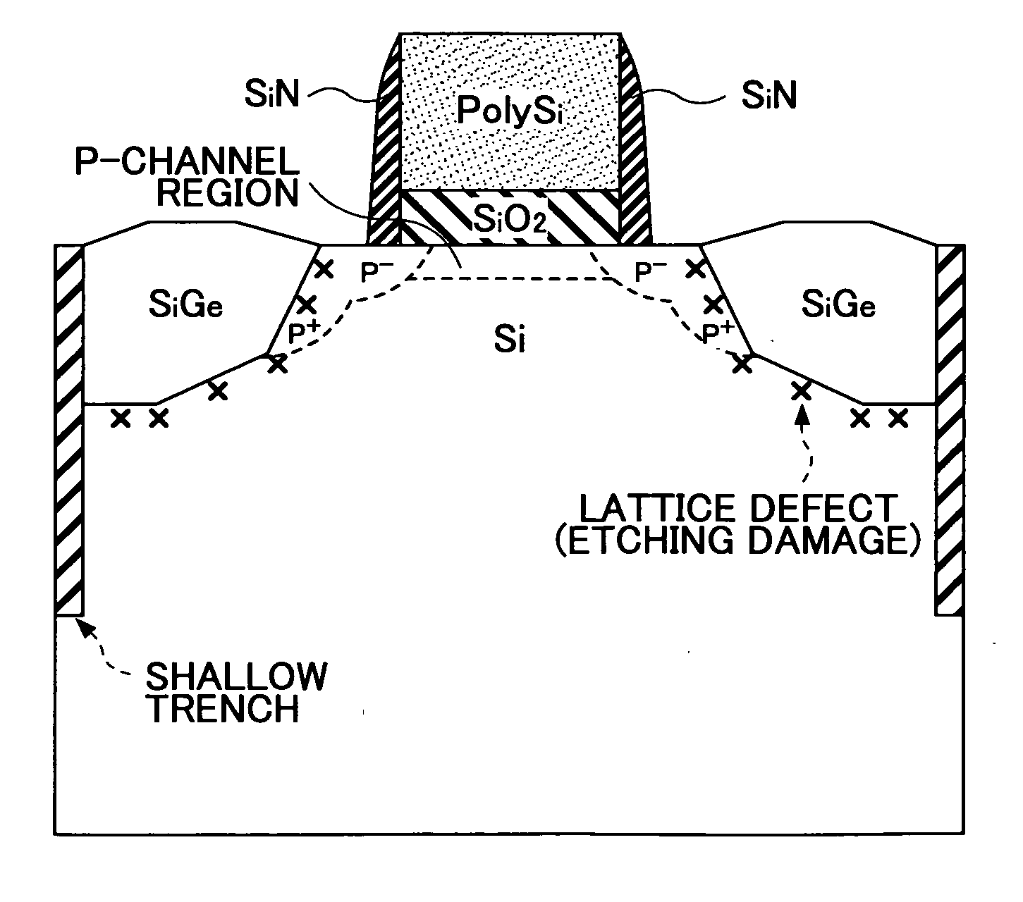
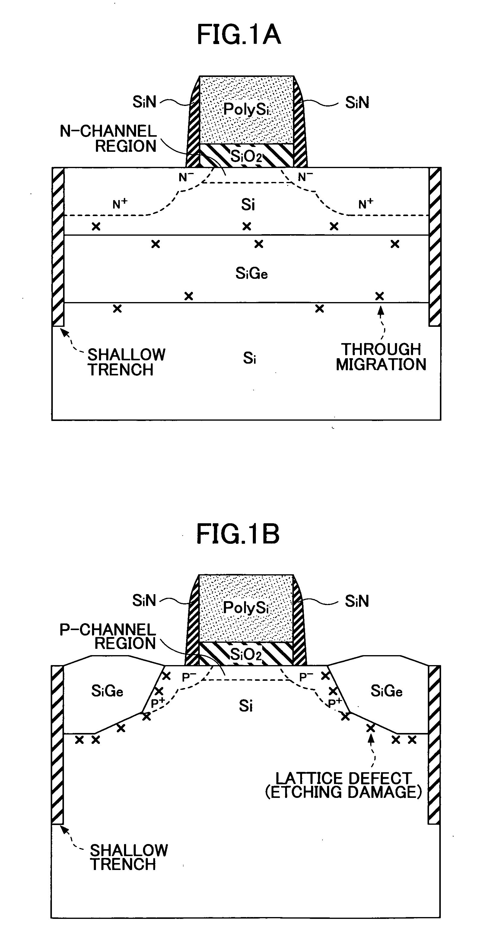
[0047]FIG. 4 is a cross-sectional view of a semiconductor device according to the first embodiment of the invention, and FIGS. 5A through 5E illustrate a semiconductor device fabrication method according the first embodiment. In the first embodiment, a semiconductor device with a p-type MOSFET is fabricated.

[0048] The semiconductor device shown in FIG. 4 comprises a silicon (Si) substrate 101, a gate insulating film 102, a gate electrode 103, and a sidewall 104. The silicon substrate 101 includes a p-channel region 111p, a source region 112, a drain region 113, and source / drain extensions (hereinafter referred to simply as “extensions”) 134.

[0049] The semiconductor device also comprises strain generating layers 121 that cause strain in the p-channel region 111p by applying a uniaxial compressive stress thereto. The strain generating layers 121 are localized strain generating layers embedded in grooves 131 (See FIG. 5D) formed one in each of the source region 112 and the drain regi...


PUM


Abstract

A semiconductor device includes a field effect transistor and a strain generating layer to apply a stress to a channel region of the field effect transistor. The strain generating layer contains at least one of oxygen and nitrogen of 1.0×1018 cm−3 to 5.0×1019 cm−3, or alternatively, the strain generating layer contains self-interstitial atoms and/or vacancies of 1.0×1018 cm−3 to 5.0×1019 cm−3. In the latter case, at least a portion of the self-interstitial atoms and/or the vacancies exist as a cluster.

Description

CROSS-REFERENCE TO A RELATED APPLICATION [0001] This is a continuation in part of U.S. application Ser. No. 11 / 167,580, filed Jun. 28, 2005.BACKGROUND OF THE INVENTION [0002] 1. Field of the Invention [0003] The present invention relates to a semiconductor device and a manufacturing method thereof. [0004] 2. Description of the Related Art [0005] Field Effect Transistors (FETs) have a characteristic in that strain in channel regions improves carrier mobility. “Strain generating techniques” for causing strain in channel regions are attracting increased interest for application to super speed FETs having a gate length of 100 nm or less. FIG. 1A illustrates an example of strain generating methods. According to this method, a silicon (Si) layer having an N-channel region is formed on the surface of a silicon-germanium (SiGe) layer. Thus, a biaxial tensile stress is applied to the N-channel to cause strain therein. FIG. 1B illustrates another example of strain generating methods. Accordin...

Claims


Application Information

Patent Timeline
Patent Type & Authority Applications(United States)
IPC IPC(8): H01L29/76
CPCH01L21/26506H01L29/1054H01L29/165H01L29/66636H01L29/78H01L29/7848A47K3/283
Inventor HARA, AKITO
Owner FUJITSU LTD
Why Eureka
Try Eureka