Laser diode chip, laser diode, and method for manufacturing laser diode chip

a laser diode and laser diode technology, applied in the direction of laser cooling arrangement, laser details, semiconductor lasers, etc., can solve the problems of high threshold current which starts laser oscillation, large astigmatic difference, and increase production cost, so as to improve the yield of the chip, reduce the threshold current, and reduce the effect of astigmatic differen

Inactive Publication Date: 2006-09-14
PHENITEC SEMICON CORP +1
View PDF3 Cites 11 Cited by
  • Summary
  • Abstract
  • Description
  • Claims
  • Application Information

AI Technical Summary

Benefits of technology

[0019] The present invention has been devised in view of such circumstances and hence, it is an object of the invention to provide a laser diode chip which outputs an infrared, red or violet laser beam, a laser diode provided with the laser diode chip, and a method for manufacturing the laser diode chip. The laser diode chip also offers other advantages not only in that a threshold current, by which laser oscillation is started, is decreased and an astigmatic difference is made small by providing current restricting layers, which have been formed by baking a liquid oxide film, so as to be opposite to each other with the central portion (stripe) of a clad layer of a p-type semiconductor, which lies substantially vertically to the direction of the lamination of the chip, interposed therebetween but in that the yield of the chip can be further improved than ever and the production cost of the chip can be reduced by eliminating the process of crystal growth twice through the provision of the current restricting layers.
[0020] Another object of the invention is to provide a laser diode chip, which is capable of confining light and carriers by increasing the thicknesses of current restricting layers with distance from the central portion (stripe) of a clad layer of a p-type semiconductor and which outputs an infrared, red, or violet laser beam, and a laser diode provided with the laser diode chip.

Problems solved by technology

Because of this, there are the disadvantages that a threshold current which starts laser oscillation is high and an astigmatic difference is large.
However, in these conventional methods, there is a necessity to repeat the process of the crystal growth plural times to form the current restricting layers, which leads to a problem in that their production cost rises.
In addition, the process of the crystal growth, which requires the precise control of layer thicknesses, often affects the yield of products, which leads to a problem in that the repetition of the process of the crystal growth results in the reduced yield of laser diode chips.

Method used


Image

  • Laser diode chip, laser diode, and method for manufacturing laser diode chip
  • Laser diode chip, laser diode, and method for manufacturing laser diode chip
  • Laser diode chip, laser diode, and method for manufacturing laser diode chip

Examples


first embodiment

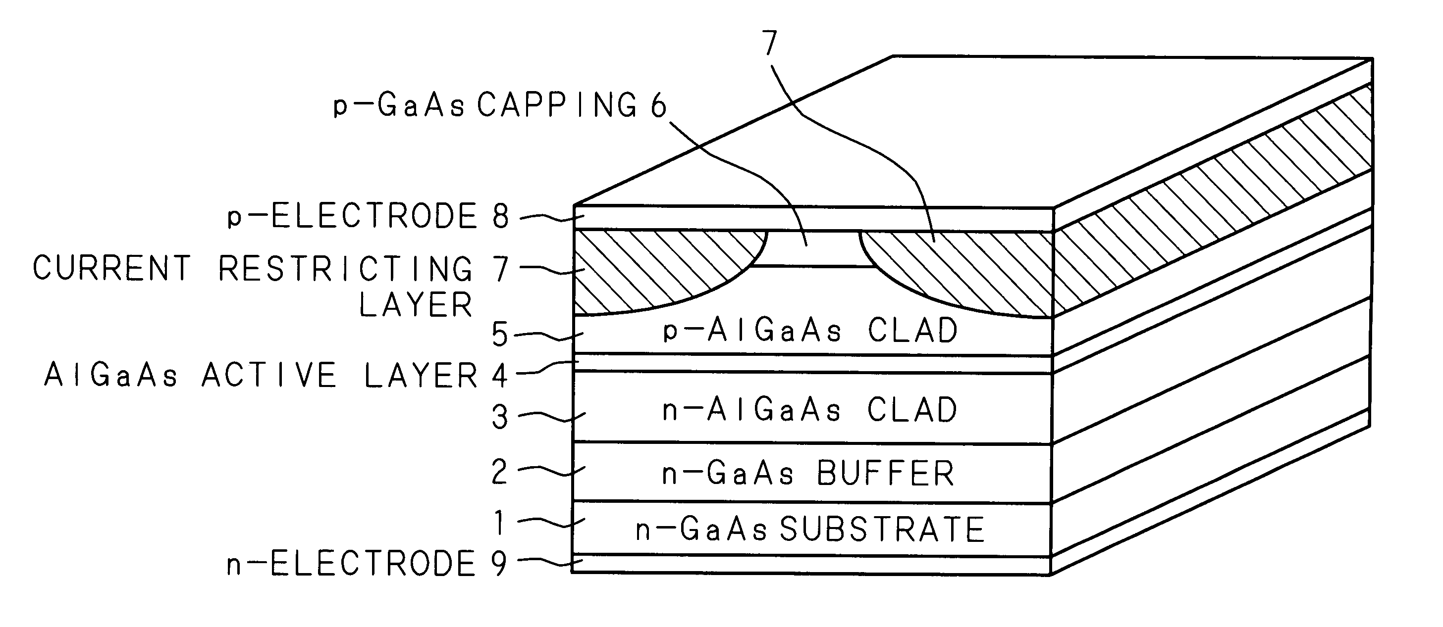
[0070]FIG. 3 is a schematic diagram of the structure of a laser diode chip according to a first embodiment of the invention. In FIG. 3, reference numeral 1 denotes a n-type GaAs substrate made of a n-type GaAs-based semiconductor crystal. The n-type GaAs substrate 1 is of the shape of, for example, a rectangular parallelepiped approximately 250 μm wide (width)×100 μm thick (height)×300 μm long.

[0071] On the n-type GaAs substrate 1, for example, an about 0.5 μm thick n-type GaAs buffer layer 2 made of n-type GaAs-based semiconductor crystal, an about 0.5 μm thick n-type AlGaAs clad layer 3 made of n-type AlGaAs-based semiconductor crystal, an about 0.06 μm thick AlGaAs active layer 4 made of AlGaAs-based semiconductor crystal, an about 0.5 μm thick p-type AlGaAs clad layer 5 made of p-type AlGaAs-based semiconductor crystal, and an about 0.5 μm thick p-type GaAs capping layer 6 made of p-type GaAs-based semiconductor crystal are laminated in that order by using epitaxial crystal gro...

second embodiment

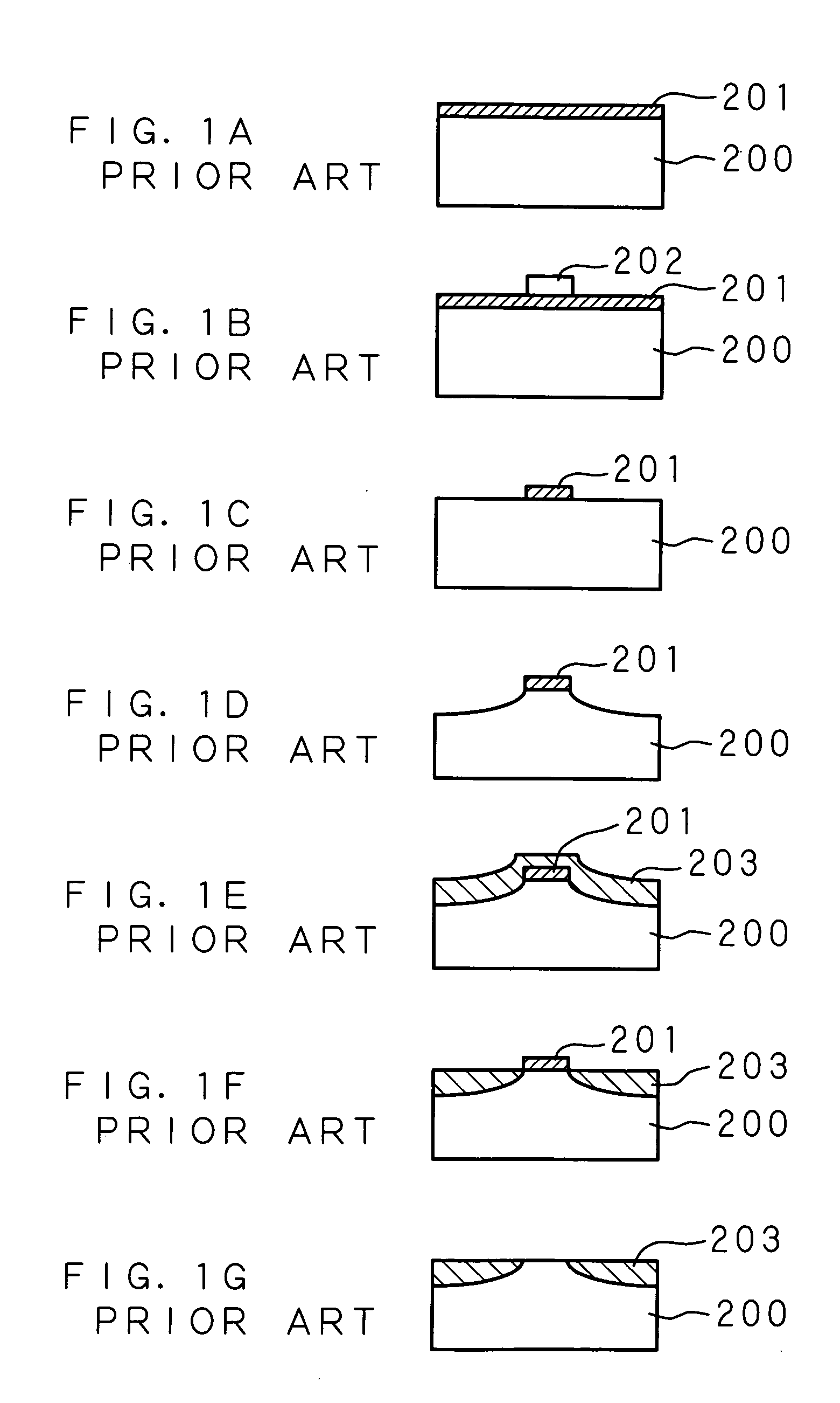
[0080] With the laser diode chip according to the first embodiment, both side portions of the p-type GaAs capping layer 6 are removed by etching, upper parts of both side portions of the p-type AlGaAs clad layer 5 are removed by etching, and then the current restricting layers 7 are provided to the cut portions; however, the structure of the current restricting layers 7 is not limited to such a structure.

[0081]FIGS. 5A and 5B are schematic diagrams of the structures of current restricting layers 7. As shown in FIG. 5A, both side portions of the p-type GaAs capping layer 6 and the p-type AlGaAs clad layer 5 are removed by etching and upper parts of both side portions of the AlGaAs active layer 4 are removed by etching. The depths in the longitudinal direction of the removed portions are increased toward the longitudinal edges of the laser diode chip. The current restricting layers 7 formed by baking a liquid oxide film are provided to the cut portions.

[0082] Also, as shown in FIG. ...

third embodiment

[0083] The laser diode chips according to the first and second embodiments of the invention has a structure in which the active layer made of the AlGaAs-based semiconductor crystal is used and outputs the infrared laser beam with a laser beam power on the order of several mW to several tens of mW And further, it is also possible to apply such a structure to a laser diode chip which outputs an infrared laser beam with a high power on the order of a hundred mW to several hundreds of mW.

[0084]FIG. 6 is a schematic diagram of the structure of a high power-type laser diode chip. In FIG. 6, reference numeral 11 denotes an about 500 Å thick MQW (multi-quantum well) active layer made by alternately laminating quantum well layers, which are extremely thin films 100 Å thick or less and which are made of AlGaAs-based semiconductor crystal, and quantum barrier layers which are extremely thin films 100 Å thick or less and which are made of GaAs-based semiconductor crystal. A p-type AlGaAs waveg...


PUM


Abstract

Both lateral side portions of a laser diode chip separated by the central portions of a p-type capping layer and a p-type clad layer and parallel to the horizontal edges of the cleavage planes of the chip are cut away by etching, so that the p-type capping layer and the p-type clad layer take the shape of a mountain in cleavage planes which are the end faces of an active layer. The cut portions are provided with current restricting layers of oxide film made by baking a liquid oxide film. The thicknesses of the current restricting layers are increased with distance from the central portion of the laser diode chip.

Description

CROSS-REFERENCE TO RELATED APPLICATIONS [0001] This Nonprovisional application claims priority under 35 U.S.C. §119(a) on Patent Applications Nos. 2005-64534, 2005-64535, 2005-64536, 2005-64537 filed in Japan on Mar. 8, 2005, the entire contents of which are hereby incorporated by reference. BACKGROUND OF THE INVENTION [0002] The present invention relates to a laser diode chip, which is comprised of a semiconductor substrate and semiconductor layers and which outputs a laser beam, a laser diode provided with the laser diode chip, and a method for manufacturing the laser diode chip. [0003] In recent days, optical disks are used to store data, such as audio data and image data, converted to digital signals. For example, with compact disks (CDs), laser diode provided with a laser diode chip, which outputs a laser beam with a wavelength of 780 nm (in the infrared region), is used for the writing and reading of data. Also, for example, with digital versatile disks (DVDs), a laser diode p...

Claims


Application Information

Patent Timeline
Patent Type & Authority Applications(United States)
IPC IPC(8): H01S5/00
CPCH01S5/2214H01S5/2231H01S5/2275H01S5/32316H01S5/32325H01S5/32333H01S5/32341H01S5/4031H01S5/4087
Inventor IMAI, YUJI
Owner PHENITEC SEMICON CORP
Why Eureka
Try Eureka