Nitride semiconductor device

Inactive Publication Date: 2006-11-02
PANASONIC CORP
View PDF3 Cites 31 Cited by
  • Summary
  • Abstract
  • Description
  • Claims
  • Application Information

AI Technical Summary

Benefits of technology

[0043] With this structure, in the semiconductor laser to which the present invention is applied, the AlGaN layer having a large Al composition is used as a cladding layer. Thus, confinement of light in the active layer is further improved and a semiconductor laser with a lower threshold current can be realized.
[0044] As has been described above, in each of the nitride semiconductor light emitting device and the nitride semiconductor photo detector device, the active layer having a periodic structure of the InAlGaN quaternary alloy crystal layer and the AlGaN layer can be formed to be a so-called type II quantum well active layer by preferably setting the respective compositions of the InAlGaN quaternary alloy crystal layer and the AlGaN layer. Thus, unlike the known example, emission of light having a long wavelength can be realized without increasing an In c

Problems solved by technology

To extend application fields of GaN based light emitting devices, longer luminescent wavelength of light emitting devices is one of technical challenges.
Thus, there arise problems with respect to crystal growth, such as crystal dislocations caused by lattice mismatch between the InGaN well layer and the GaN layer and In segr

Method used


Image

  • Nitride semiconductor device
  • Nitride semiconductor device
  • Nitride semiconductor device

Examples


first embodiment

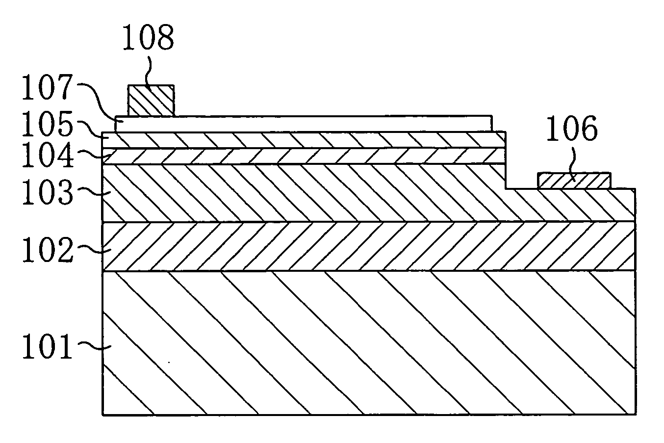
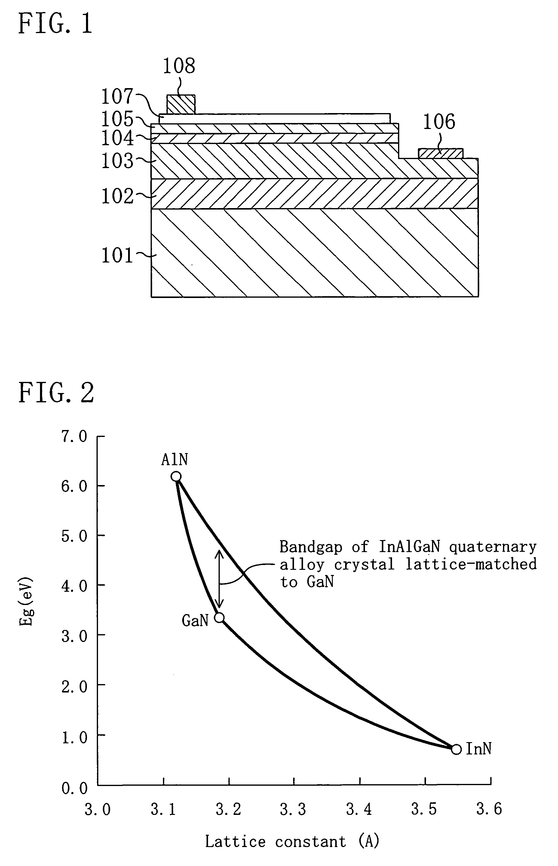
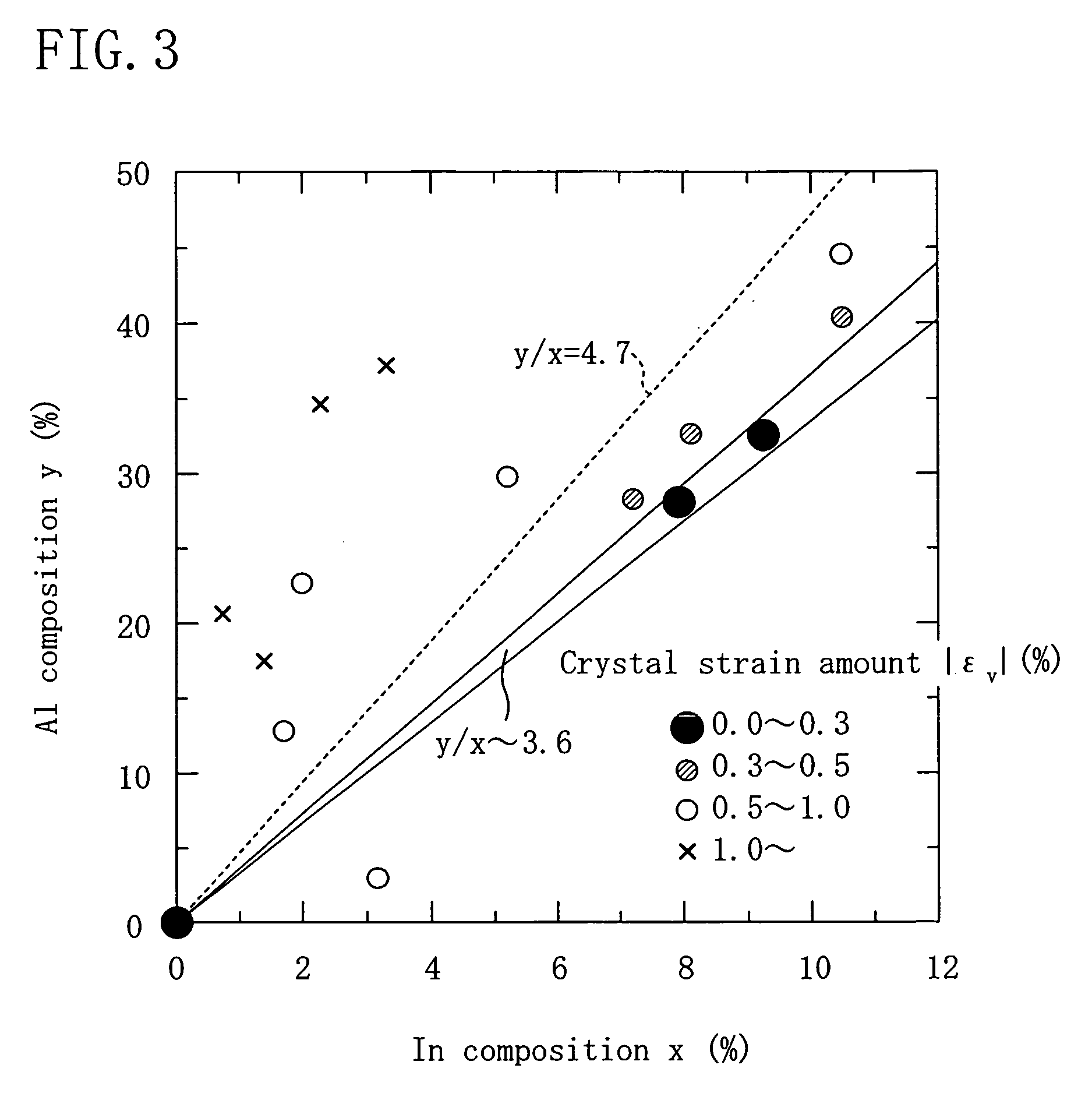
[0057] Hereafter, a first embodiment of the present invention will be described with reference to FIGS. 1 through 7. FIG. 1 is a cross-sectional view illustrating a structure of a nitride semiconductor light emitting device according to the first embodiment of the present invention. FIG. 2 is a graph showing a bandgap of InAlGaN quaternary alloy crystal which is lattice-matched to GaN and used in the present invention and the relationship between lattice constant and bandgap for nitride semiconductor. FIG. 3 is a graph obtained by plotting y / x values of InxA1yGa1−x−yN quaternary alloy crystals which have been classified by respective crystal strain amounts thereof. The InxAlyGa1−x−yN quaternary alloy crystals were obtained by actual crystal growth of InxAlyGa1−x−yN quaternary alloy crystals having different compositions on GaN actually conducted by the present inventors. FIG. 4 is a graph showing the dependency of bandgap on In composition for InAlGaN quaternary alloy crystal when I...

second embodiment

[0069] Hereafter, a second embodiment of the present invention will be described with reference to FIGS. 8 thorough 9. FIG. 8 is a cross-sectional view illustrating a structure of a nitride semiconductor light emitting device according to the second embodiment of the present invention. FIG. 9 is a graph showing a band diagram of active layer part of the nitride semiconductor light emitting device according to the second embodiment of the present invention. In FIG. 8, 201 denotes an R plane sapphire substrate, 202 denotes an n-type GaN layer, 203 denotes an n-type Al0.1Ga0.9N cladding layer, 204 denotes an In0.07Al0.33Ga0.6N / Al0.04Ga0.96N multiple quantum well active layer, 205 denotes a p-type Al0.1Ga0.9N cladding layer, 206 denotes a Ti / Al / Ni / Au electrode, 207 denotes a Ni / Au transparent electrode and 208 denotes an Au electrode.

[0070] In this embodiment, a nitride semiconductor layer having a surface of an a plane, i.e., (11-20) plane is epitaxially grown on a sapphire substrate ...


PUM


Abstract

A nitride semiconductor device includes an active layer including a first nitride semiconductor layer and a second nitride semiconductor layer which are periodically stacked, the second nitride semiconductor layer having a different composition from a composition of the first nitride semiconductor layer. An energy at a lower edge of a conduction band in the first nitride semiconductor layer is lower than an energy at a lower edge of a conduction band in the second nitride semiconductor layer, and an energy at an upper edge of a valence band in the first nitride semiconductor layer is lower than an energy at an upper edge of a valence band in the second nitride semiconductor layer.

Description

CROSS-REFERENCE TO RELATED APPLICATION [0001] The disclosure of Japanese Patent Applications No. 2005-129301 filed on Apr. 27, 2005 and No. 2006-115155 including specification, drawings and claims are incorporated herein by reference in its entirety. BACKGROUND OF THE INVENTION [0002] The present invention relates to a nitride semiconductor device such as a nitride semiconductor light emitting device applicable to, for example, a short wavelength light emitting diode or a blue-violet semiconductor laser and a nitride semiconductor photo detector device capable of receiving visible light or ultraviolet light. [0003] GaN based group III-V nitride semiconductor (which will be hereafter referred to as merely “nitride semiconductor”) have a large bandgap, i.e., 3.4 eV at room temperature in GaN, and a pn junction or double hetero junction structure can be easily formed. For this reason, nitride semiconductor is applicable to light emitting devices such as a visible region light emitting ...

Claims


Application Information

Patent Timeline
IPC IPC(8): H01L33/00H01L33/06H01L33/32
CPCB82Y20/00H01L31/0304H01L31/03046H01L31/035236Y02E10/544H01L33/06H01L33/32H01S5/322H01S5/34333H01L31/1035
Inventor UEDA, TETSUZONAKAZAWA, SATOSHIUEDA, DAISUKETAKIZAWA, TOSHIYUKI
Owner PANASONIC CORP
Why Eureka
Try Eureka