Hybrid Waveguide Lasers and Methods for Fabricating Hybrid Waveguide Lasers

a laser and hybrid technology, applied in semiconductor lasers, instruments, optical elements, etc., can solve the problems of increasing the number of lasers required per chip, and increasing the cost of die bonding or wafer bonding methods, so as to achieve sufficient high quality and improve the confinement of ligh

Active Publication Date: 2015-11-19
INTERUNIVERSITAIR MICRO ELECTRONICS CENT (IMEC VZW) +1
View PDF3 Cites 13 Cited by
  • Summary
  • Abstract
  • Description
  • Claims
  • Application Information

AI Technical Summary

Benefits of technology

[0011]According to embodiments of the present disclosure, sufficiently small waveguide lasers can be made so that epitaxial growth of layers with a sufficient high quality can be obtained while at the same time leakage, which typically is considered a major problem in small waveguide lasers, can be controlled.
[0012]It should be noted that within the context of this application the term “light confinement element” may be any type of element or feature that allows improving the confinement of light in the channel waveguide (such as in the active region), e.g., that allows increasing the amount of light kept within the sub-micron channel waveguide, e.g., within the active region of the sub-micron channel waveguide. The light confinement element may be provided adjacent to the channel waveguide.
[0013]It also should be noted that within the context of this disclosure the term local-epitaxy-grown refers to materials that are grown by epitaxial deposition, whereby the deposition is substantially limited to the specific area where the layer should be grown, which helps to avoid depositing too much material that should be removed afterwards, as well as to avoid additional patterning of the epitaxial material grown after the deposition.

Problems solved by technology

Tight mechanical alignment requirements may make this option less attractive for wavelength division multiplexing (WDM) systems, wherein the number of lasers required per chip has increased over the years.
However, using a die bonding or wafer bonding approach is relatively expensive.
However, this approach results in a relatively high fabrication cost due the rather large consumption of expensive III-V semiconductor materials.

Method used


Image

  • Hybrid Waveguide Lasers and Methods for Fabricating Hybrid Waveguide Lasers
  • Hybrid Waveguide Lasers and Methods for Fabricating Hybrid Waveguide Lasers
  • Hybrid Waveguide Lasers and Methods for Fabricating Hybrid Waveguide Lasers

Examples


Embodiment Construction

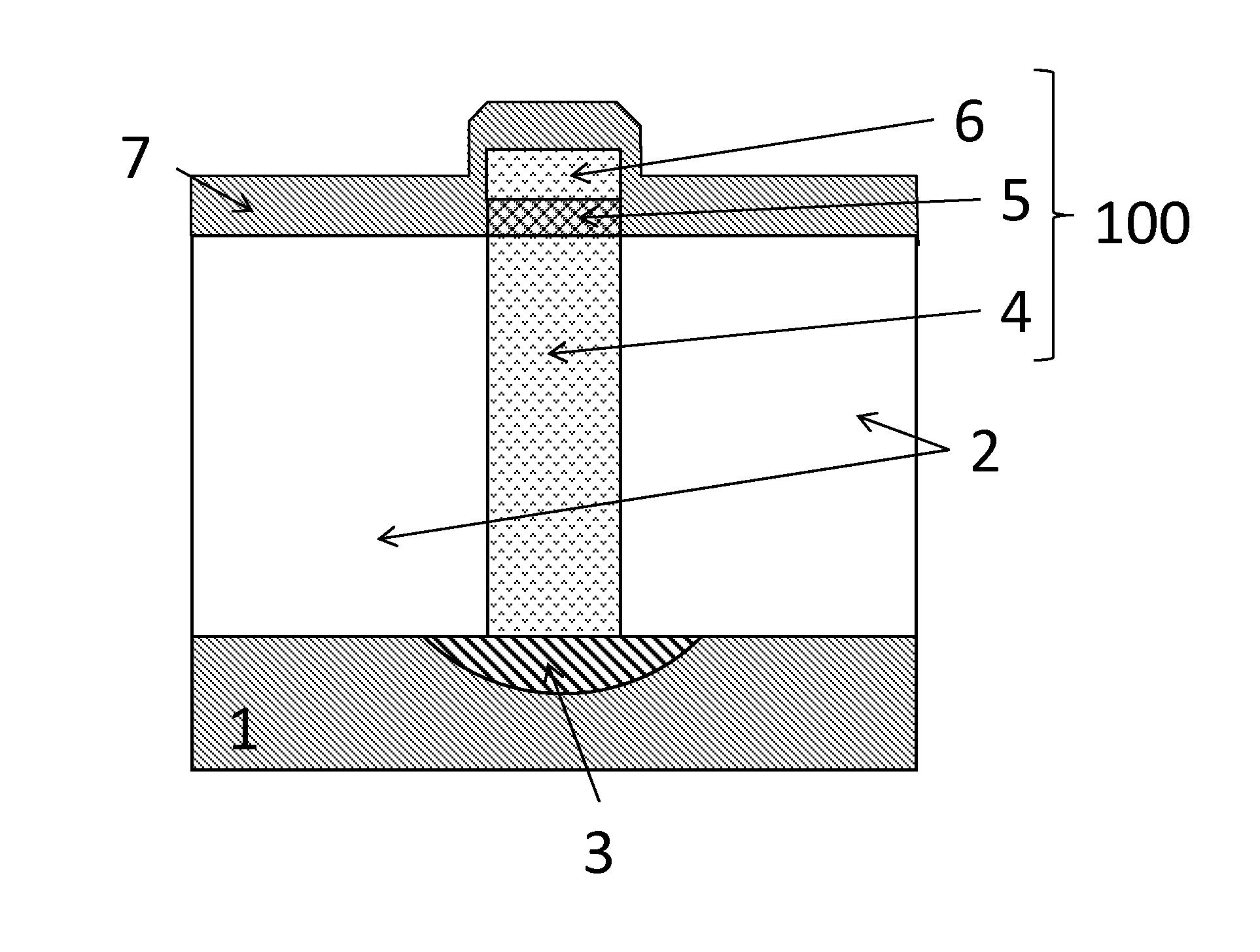
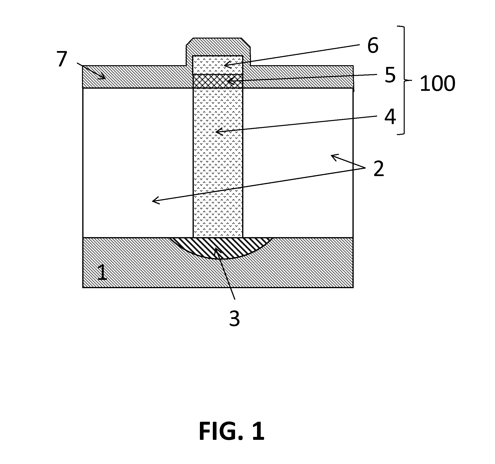
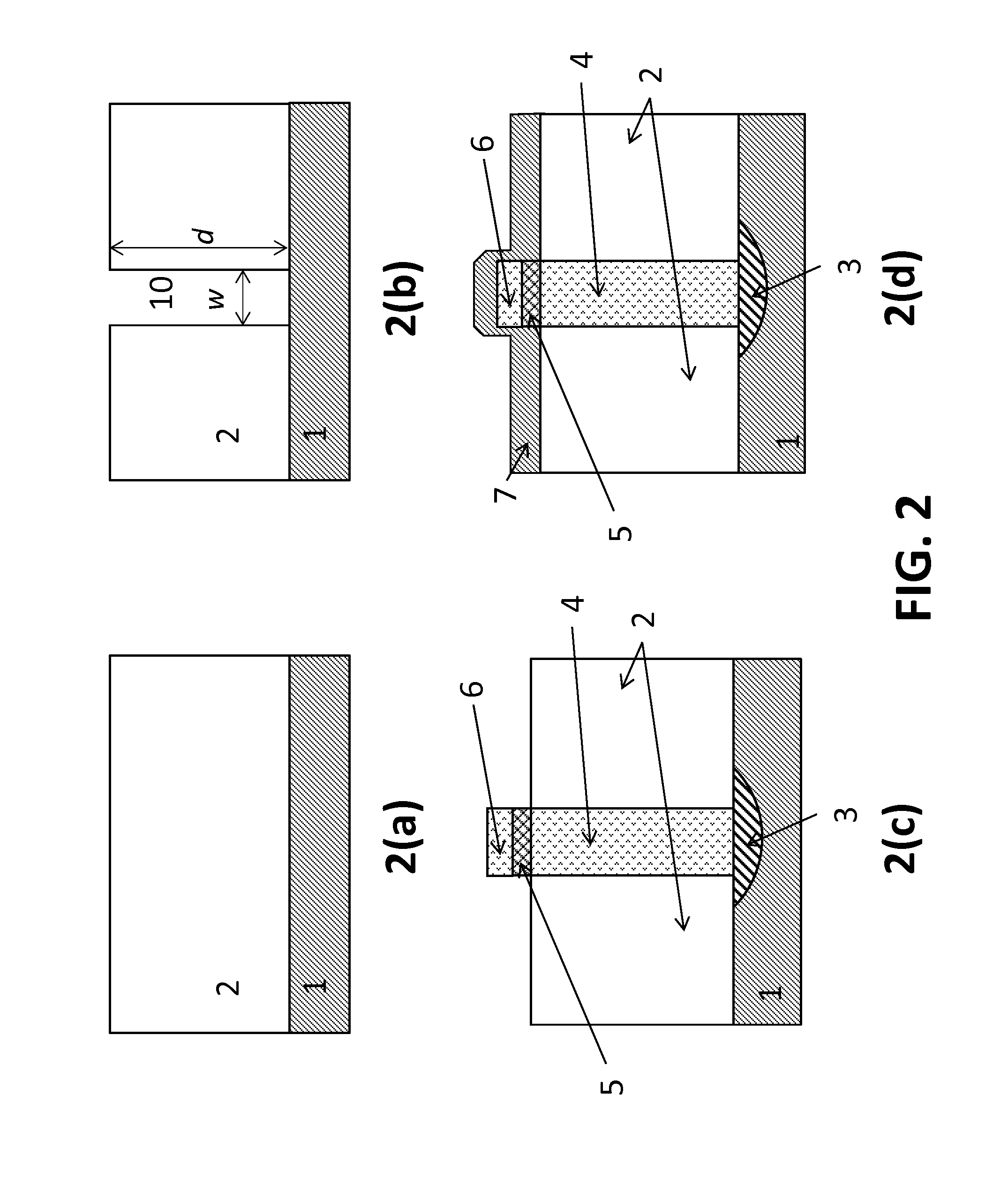
[0039]In the following detailed description, numerous specific details are set forth in order to provide a thorough understanding of the disclosure and how it may be practiced in particular embodiments. However, it will be understood that the present disclosure may be practiced without these specific details. In other instances, well-known methods, procedures and techniques have not been described in detail, so as not to obscure the present disclosure. While the present disclosure will be described with respect to particular embodiments and with reference to certain drawings, the disclosure is not limited hereto. The drawings included and described herein are schematic and are not limiting the scope of the disclosure.

[0040]The present disclosure will be described with respect to particular embodiments and with reference to certain drawings but the disclosure is not limited thereto but only by the claims. The drawings described are only schematic and are non-limiting. In the drawings...


PUM


Abstract

The present disclosure relates to a method for integrating a sub-micron III-V waveguide laser on a semiconductor photonics platform as well as to a corresponding device/system. The method comprises providing on a semiconductor substrate an electrically insulating layer, etching a trench having a width in the range between 50 nm and 800 nm through the electrically insulating layer, thereby locally exposing the silicon substrate, providing a III-V layer stack in the trench by local epitaxial growth to form a channel waveguide, and providing a light confinement element for confining radiation in the local-epitaxial-grown channel waveguide.

Description

CROSS-REFERENCE TO RELATED APPLICATION[0001]This application claims priority to European Patent Application No. 13174582.0 filed on Jul. 1, 2013, the contents of which are hereby incorporated by reference.FIELD OF THE DISCLOSURE[0002]The disclosed technology relates to hybrid waveguide lasers, e.g., sub-micron hybrid waveguide lasers, and to methods for integrating such waveguide lasers on a semiconductor platform, such as, for example, a silicon photonics platform.BACKGROUND OF THE DISCLOSURE[0003]Driven by demands from optical I / O, telecommunications, optical computing, and other applications, extensive research is being carried out in the field of integrating III-V semiconductor devices on silicon. Various options have been suggested for integrating electrically pumped lasers and optical amplifiers on a silicon based photonics platforms.[0004]Individual laser dies may be flip chip mounted to a silicon photonics wafer or may be transferred to a silicon platform using an epitaxial ...

Claims


Application Information

Patent Timeline
Patent Type & Authority Applications(United States)
IPC IPC(8): H01S5/20H01S5/02H01S5/30H01S5/022H01S5/042H01S5/02315
CPCH01S5/2077H01S5/02236H01S5/0203H01S5/3013H01S5/042H01S5/021H01S5/026H01S5/2027H01S5/2214H01S5/2218H01S5/2272H01S2301/176G02B6/12004G02B6/1228G02B2006/12078G02B2006/12121H01S5/02315H01S5/0233H01S5/0235
Inventor VAN THOURHOUT, DRIESWANG, ZHECHAOVAN CAMPENHOUT, JORISPANTOUVAKI, MARIA IOANNA
Owner INTERUNIVERSITAIR MICRO ELECTRONICS CENT (IMEC VZW)
Why Eureka
Try Eureka