Semiconductor device and manufacturing method thereof

a semiconductor and semiconductor technology, applied in the field of semiconductor devices, can solve the problems of reducing reducing the efficiency of emitter injection, and affecting the production efficiency of semiconductor/solid-state devices, so as to reduce the current gain bfe, reduce the emitter injection efficiency, and the effect of high withstanding voltag

Inactive Publication Date: 2006-09-21
NISSAN MOTOR CO LTD
View PDF3 Cites 6 Cited by
  • Summary
  • Abstract
  • Description
  • Claims
  • Application Information

AI Technical Summary

Benefits of technology

[0008] It is required for realizing a high withstanding voltage to prevent punch-through, which is a phenomenon that, due to the reverse voltage applied to a collector electrode, a depletion layer is expanded in a p-type base region to reach an n+-type emitter region. For this purpose, the space charge density of the depletion layer has to be increased within the p-type base region in order not to inhibit the expansion of the depletion layer. However, when the space charge density increases, the free carrier density in the p-type base region also increases to decrease the emitter injection efficiency and therefore decrease the current gain bFE. As a result, a larger base current is required for controlling the collector current.

Problems solved by technology

However, when the space charge density increases, the free carrier density in the p-type base region also increases to decrease the emitter injection efficiency and therefore decrease the current gain bFE.
That is, there is a problem that a tradeoff exists between the withstanding voltage of the device and the current gain hFE.

Method used


Image

  • Semiconductor device and manufacturing method thereof
  • Semiconductor device and manufacturing method thereof
  • Semiconductor device and manufacturing method thereof

Examples


embodiment 1

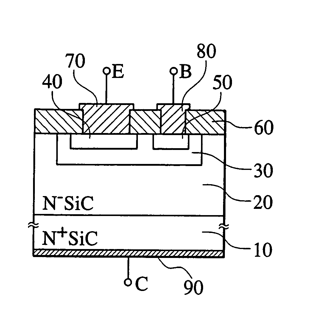
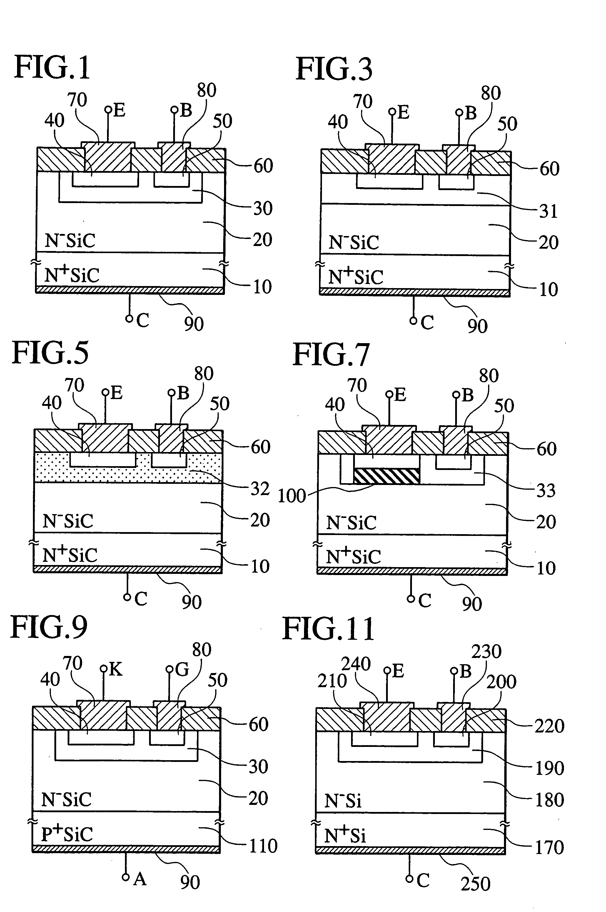
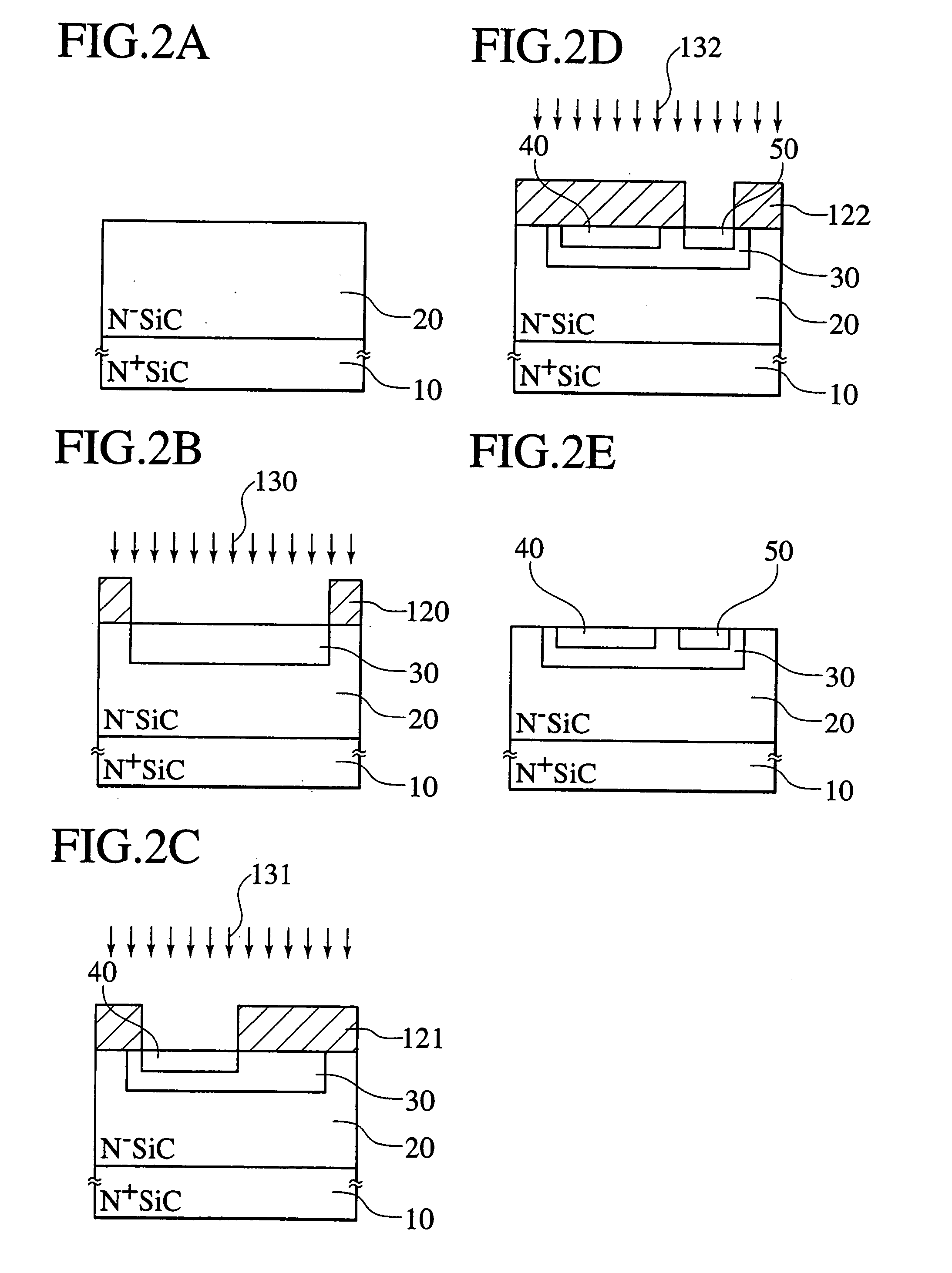
[0034]FIG. 1 is a cross sectional view showing the structure of an embodiment 1 of the semiconductor device in accordance with the invention.

[0035] The present embodiment 1 is applicable to a high voltage SiC semiconductor bipolar transistor in which a p-type base region is formed with boron as a dopant

[0036] The high voltage SiC semiconductor device comprises an n−-type epitaxial layer 20 formed on an n+-type SiC substrate 10 in order to provide a collector region therein and a p-type base region 30 formed within a preselected surface area of the n−-type epitaxial layer 20.

[0037] The p-type base region 30 is doped with boron, which serves to generate a deep impurity level in the silicon carbide semiconductor, and has the free carrier density which is smaller than the space charge density of the depletion layer formed in the p-type base region 30 by about two orders of magnitude. In accordance with O. Takemura, T. Kimoto, H. Matsunami, T. Nakata, M. Watanabe and M. Inoue, Materia...

embodiment 2

[0091]FIG. 3 is a cross sectional view showing the structure of an embodiment 2 of the semiconductor device in accordance with the invention.

[0092] The present embodiment 2 is applicable to a high voltage SiC semiconductor bipolar transistor in which a p-type base region is formed with boron as a dopant.

[0093] The high voltage SiC semiconductor device comprises an n−- epitaxial layer 20 formed on an n+-type SiC substrate 10 in order to provide a collector region therein, and an epitaxial layer which is formed on the n−- epitaxial layer 20 in order to provide a p-type base region 31.

[0094] The high voltage SiC semiconductor device further comprises an n+-type emitter region 40 and a p+-type base contact region 50 in the predetermined areas of the surface layer of the p-type base region 31. The n+-type emitter region 40 is connected to an emitter electrode 70. Also, the p+-type base contact region 50 is connected to a base electrode 80 while a collector electrode 90 is formed on th...

embodiment 3

[0107]FIG. 5 is a cross sectional view showing the structure of an embodiment 3 of the silicon carbide semiconductor device in accordance with the invention.

[0108] The present embodiment 3 is applicable to an SiC high voltage bipolar transistor in which a p-type base region is formed with boron and aluminum as dopants.

[0109] The SiC high voltage bipolar transistor comprises an n−- epitaxial layer 20 formed on an n+-type SiC substrate 10 in order to provide a collector region therein, and an epitaxial layer which is formed on the n−- epitaxial layer 20 in order to provide a p-type base region 32.

[0110] This p-type base region 32 is formed by epitaxial growth with an impurity (boron in this case) which serves to generate a deep impurity level to form the epitaxial layer to be a p-type region, followed by ion-implantation with an impurity (aluminum in this case) which serves to generate a shallow impurity level into the entirety of the p-type region.

[0111] The high voltage SiC semi...


PUM


Abstract

A high voltage semiconductor device having a high current gain hFE is formed with a collector region (20) of a first conduction type, an emitter region (40) of the first conduction type, and a base region (30) of a second conduction type opposite to the first conduction type located between the collector region and the emitter region. The free carrier density of the base region (30) where no depletion layer is formed is smaller than the space charge density of a depletion layer formed in the base region (30).

Description

BACKGROUN OF THE INVENTION [0001] 1. Field of the Art [0002] This invention relates to a semiconductor device and a manufacturing method thereof. [0003] 2. Description of the Related Art [0004] In recent years, the research of semiconductor devices has been increasingly conducted by use of the very chemically stable nature of silicon carbide (SiC). Silicon carbide has a larger energy gap Eg, as compared with silicon, for example, Eg=3.3 eV in the case of 4H type crystals, to have a high withstanding voltage and therefore expected to be applied to power devices such as an electric power controlling device. [0005] An exemplary SiC bipolar transistor comprises a high-concentration n+-type SiC substrate on which are laminated the n−-type epitaxial region, a p-type base region, and the p+-type contact region in this order. The topmost p+-type contact region is partially removed to expose part of the p-type base region located thereunder. An n+-type emitter region is formed in the surface...

Claims


Application Information

Patent Timeline
Patent Type & Authority Applications(United States)
IPC IPC(8): H01L31/0312H01L21/331H01L21/00H01L21/265H01L29/732H01L29/74
CPCH01L29/1004H01L29/1608H01L29/6606H01L29/66068H01L29/66234H01L29/7322H01L29/861
Inventor KANEKO, SAICHIROUHOSHI, MASAKATSUMURAKAMI, YOSHINORIHAYASHI, TETSUYATANAKA, HIDEAKI
Owner NISSAN MOTOR CO LTD
Why Eureka
Try Eureka