Method for manufacturing junction semiconductor device

a semiconductor device and manufacturing method technology, applied in the direction of semiconductor devices, electrical devices, transistors, etc., can solve the problems of difficult manufacturing, difficult to obtain a normally-off characteristic, and difficult to produce width, so as to reduce the recombination state, reduce the resistance, and improve the effect of electric current amplification factor

Active Publication Date: 2006-09-28
SHINDENGEN ELECTRIC MFG CO LTD
View PDF8 Cites 5 Cited by
  • Summary
  • Abstract
  • Description
  • Claims
  • Application Information

AI Technical Summary

Benefits of technology

[0018] In accordance with the present invention, a gate region is formed using relatively low energy ion implantation in a surface that has been etched in advance to a height between the upper surface of the channel-doped layer and the lower surface of the source layer, in contrast to the conventional method for manufacturing a junction transistor. It is thereby possible to reduce the recombination states caused by crystal defects that are pr

Problems solved by technology

Additionally, with this JFET, in order to set the normally-off characteristic (non-conductive state) when voltage is not applied to the gate electrode 118, the width of the source must be made less than 1.95 μm, and such a width is very difficult to produce.
In the case of the SIT shown in FIG. 8, since the gate region is formed by high energy (MeV) injection, a considerable amount of recombination occurs via the recombination states created by ion implantation when the minority carrier is injected from the gate electrode, and the characteristics do not improve in bipolar mode operation that modulates conductivity in the high-resistance layer between the drain and the source.
Also, since channel doping is not adopted in the structure, it is very difficult to obtain a normally-off characteristic.
In order to obtain a normally-off characteristic in the case of the JFET shown in FIG. 9, a very small trench structure wi

Method used


Image

  • Method for manufacturing junction semiconductor device
  • Method for manufacturing junction semiconductor device
  • Method for manufacturing junction semiconductor device

Examples


Embodiment Construction

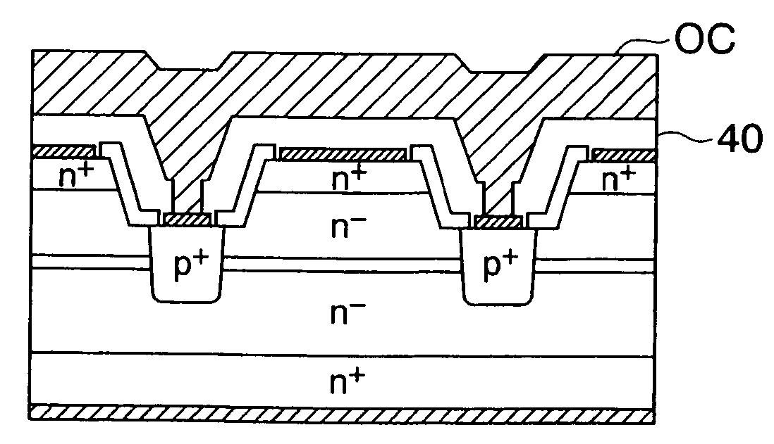
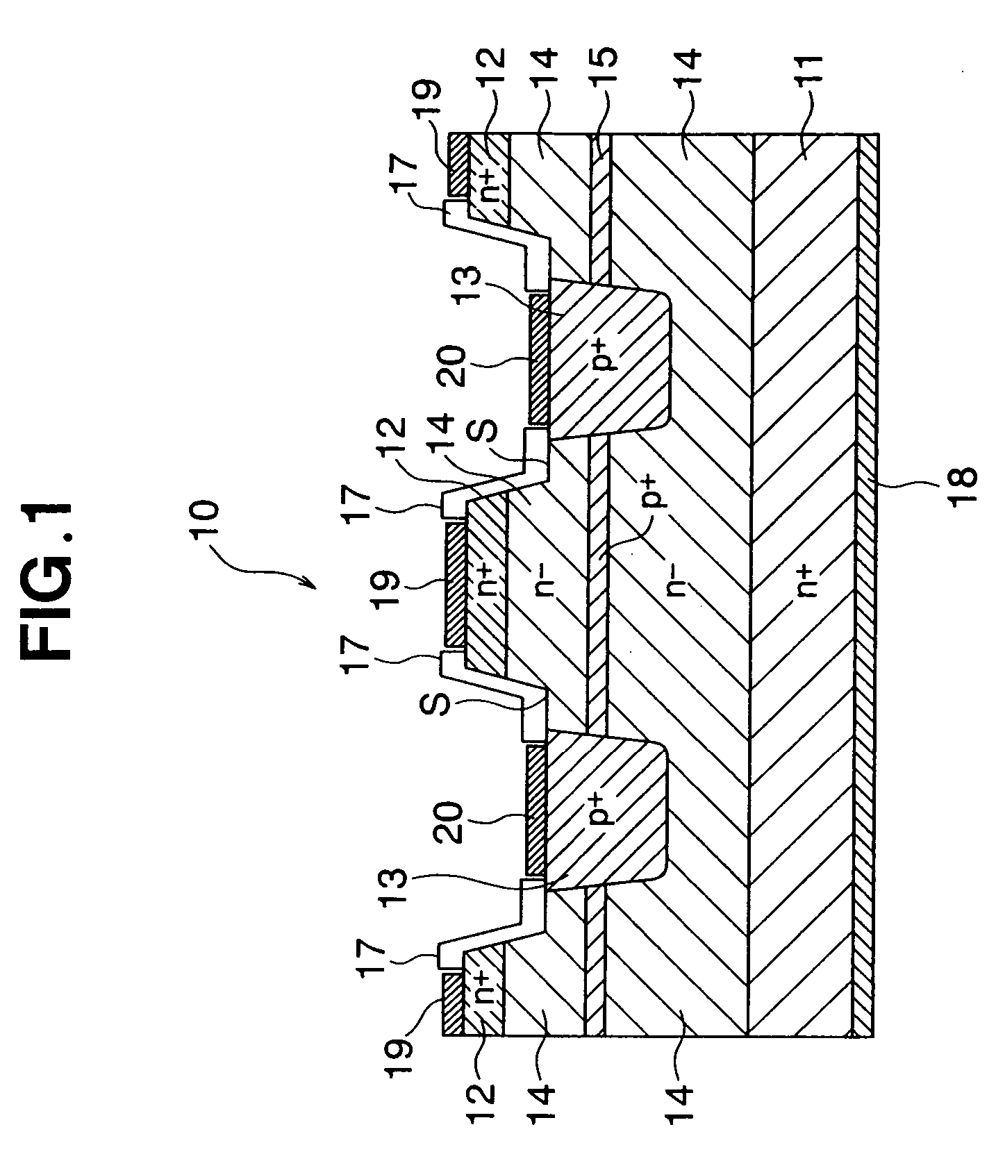
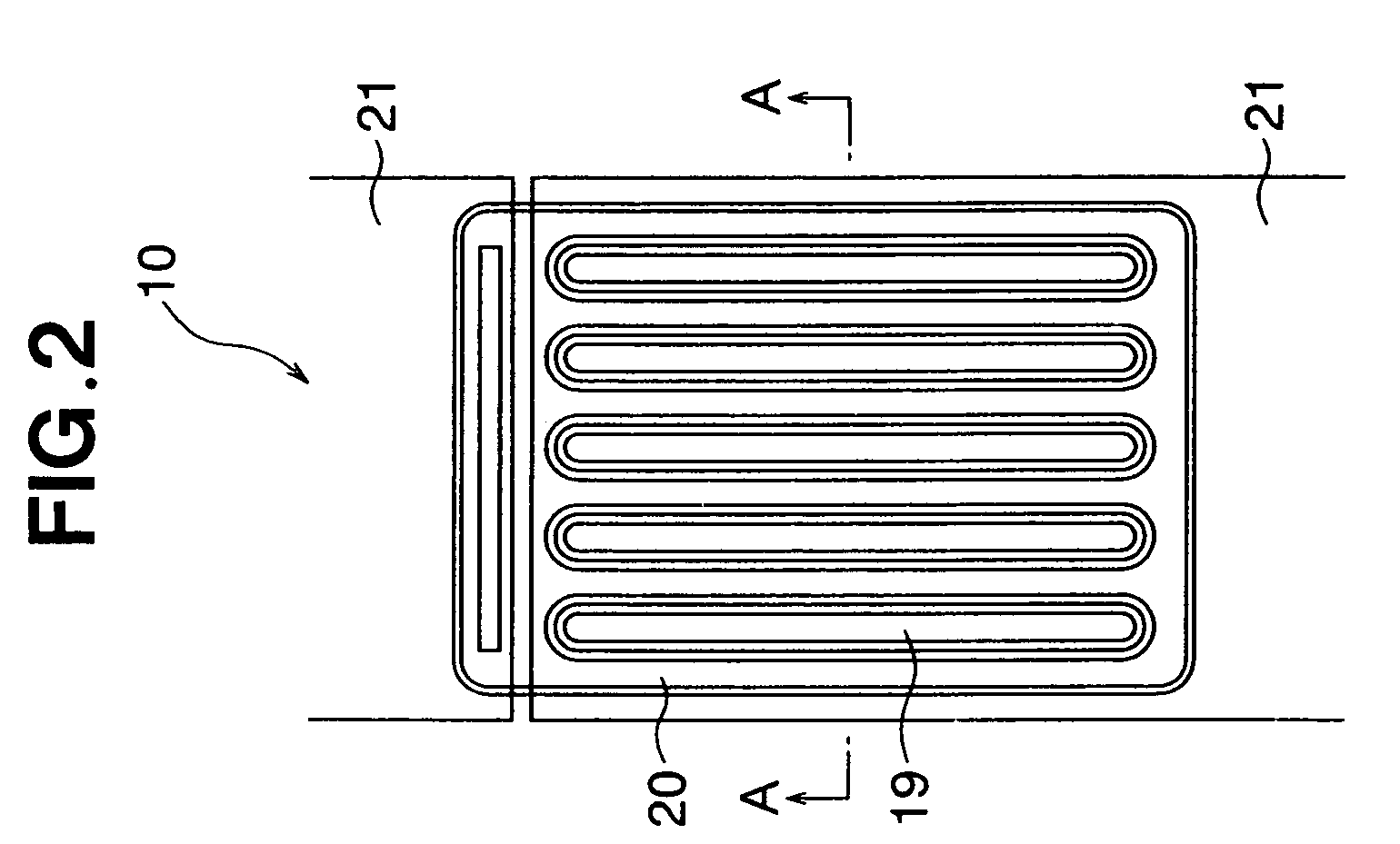
[0035]FIG. 1 is a structural cross-sectional diagram of a portion of the junction semiconductor device (static induction transistor (SIT) as an example) of the embodiments of the present invention, and FIG. 2 is a top view of the same. FIG. 2 shows an example of a static induction transistor having five source electrodes, and FIG. 1 shows an enlarged view of the structure of a single source electrode along the cross section A-A in FIG. 2. Disposed in a static induction transistor 10 are a drain area 11 composed of an n-type (first conductive type) low-resistance layer (n+ layer) formed on one surface of a silicon carbide (SiC) crystal, a source region 12 composed of an n-type low-resistance layer (n+ layer) formed on the other surface of the SiC crystal, a p-type (second conductive type) gate region 13 formed around the periphery of the source region 12, an n-type high-resistance layer (n− layer) 14 disposed between the source region 12 and the drain region 11, and a p-type channel-...


PUM


Abstract

A method for manufacturing a junction semiconductor device, having a step for forming a first high-resistance layer, a step for forming a channel-doped layer, a step for forming a second high-resistance layer, a step for forming a low-resistance layer of a first conductive type that acts as a source region, a step for performing partial etching to a midway depth of the second high-resistance layer and the low-resistance layer, a step for forming a gate region below the portion etched in the etching step, and a step for forming a protective film on the surface of the region between the gate region and the source region. A gate region is formed using relatively low energy ion implantation in the surface that has been etched in advance to a height that is between the lower surface of the source area and the upper surface of the channel-doped layer.

Description

FIELD OF THE INVENTION [0001] The present invention relates to a method for manufacturing a junction semiconductor device, and more specifically relates to a method for manufacturing a static induction transistor and other junction semiconductor devices. BACKGROUND OF THE INVENTION [0002] Semiconductor silicon carbide (SiC) has considerable bandgap energy in comparison with silicon that is widely used in devices, and is suitable for high voltage, high power, and high temperature operation. There are high expectations for its application to power devices and other components. The structure of SiC power devices, for which research and development are being actively carried out, can mainly be divided into two classes: MOS devices and junction devices. The present invention relates to a performance improvement in static induction transistors (SIT), junction field effect transistors (JFET), and other junction transistors. [0003] Following are reported examples of SITs and JFETs in which ...

Claims


Application Information

Patent Timeline
IPC IPC(8): H01L21/337
CPCH01L29/7722H01L29/80
Inventor NONAKA, KEN-ICHIHASHIMOTO, HIDEKIYOKOYAMA, SEIICHIIWANAGA, KENSUKESAITO, YOSHIMITSUIWAKURO, HIROAKISHIMIZU, MASAAKIFUKUDA, YUSUKENISHIKAWA, KOICHIMAEYAMA, YUSUKE
Owner SHINDENGEN ELECTRIC MFG CO LTD
Why Eureka
Try Eureka