Method of forming film and film forming apparatus

a film and film forming technology, applied in the direction of coatings, transistors, chemical vapor deposition coatings, etc., can solve the problems of gate oxide film disadvantageous increase, uncontrollable increase of leakage current, grain boundary leakage current, etc., to achieve suppressed leakage current, high crystallization temperature, and easy removal of silicon conten

Inactive Publication Date: 2006-09-28
TOKYO ELECTRON LTD
View PDF11 Cites 12 Cited by
  • Summary
  • Abstract
  • Description
  • Claims
  • Application Information

AI Technical Summary

Benefits of technology

[0014] According to the present invention, a hafnium compound film containing silicon (hafnium silicate film) can be obtained. Due to the anti-crystallization effect of silicon, the hafnium compound film having a high crystallization temperature can be obtained. Thus, when the hafnium compound film is exposed to a high temperature atmosphere in a succeeding process, for example, crystallization of the film can be restrained. Accordingly, the leak current can be suppressed when a voltage is applied thereto. Further, a silane-series gas such as monosilane gas and disilane gas is used as a source of silicon, the silicon content can be easily, optionally adjusted by adjusting a supply amount of the gas.

Problems solved by technology

However, when the thickness of a silicon oxide (SiO2) film, which has been conventionally used as a gate oxide film, is reduced, the leak current is undesirably increased to a considerable degree.
However, when a hafnium oxide film is exposed to a high temperature even for a short period, a part thereof is crystallized, which results in leakage of current through grain boundaries.
Thus, the leakage current of the gate oxide film is disadvantageously increased.
However, if an organic material is used as a silicon source, an amount of carbon contained in a hafnium silicate film increases.
It causes disadvantages such as an increase of the fixed charge, and deterioration in reliability and the withstand voltage of the device.
In addition, since the silicon content in the film depends on the mixing ratio of the liquid organic compound, the mixing ratio may be incompatible with other process conditions.

Method used


Image

  • Method of forming film and film forming apparatus
  • Method of forming film and film forming apparatus
  • Method of forming film and film forming apparatus

Examples


example 1

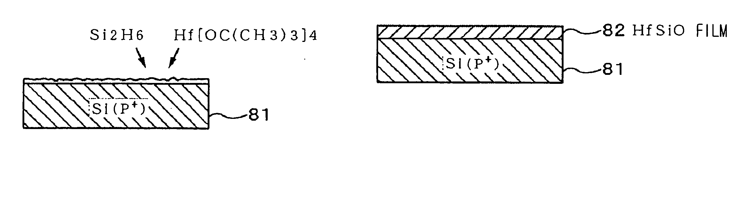
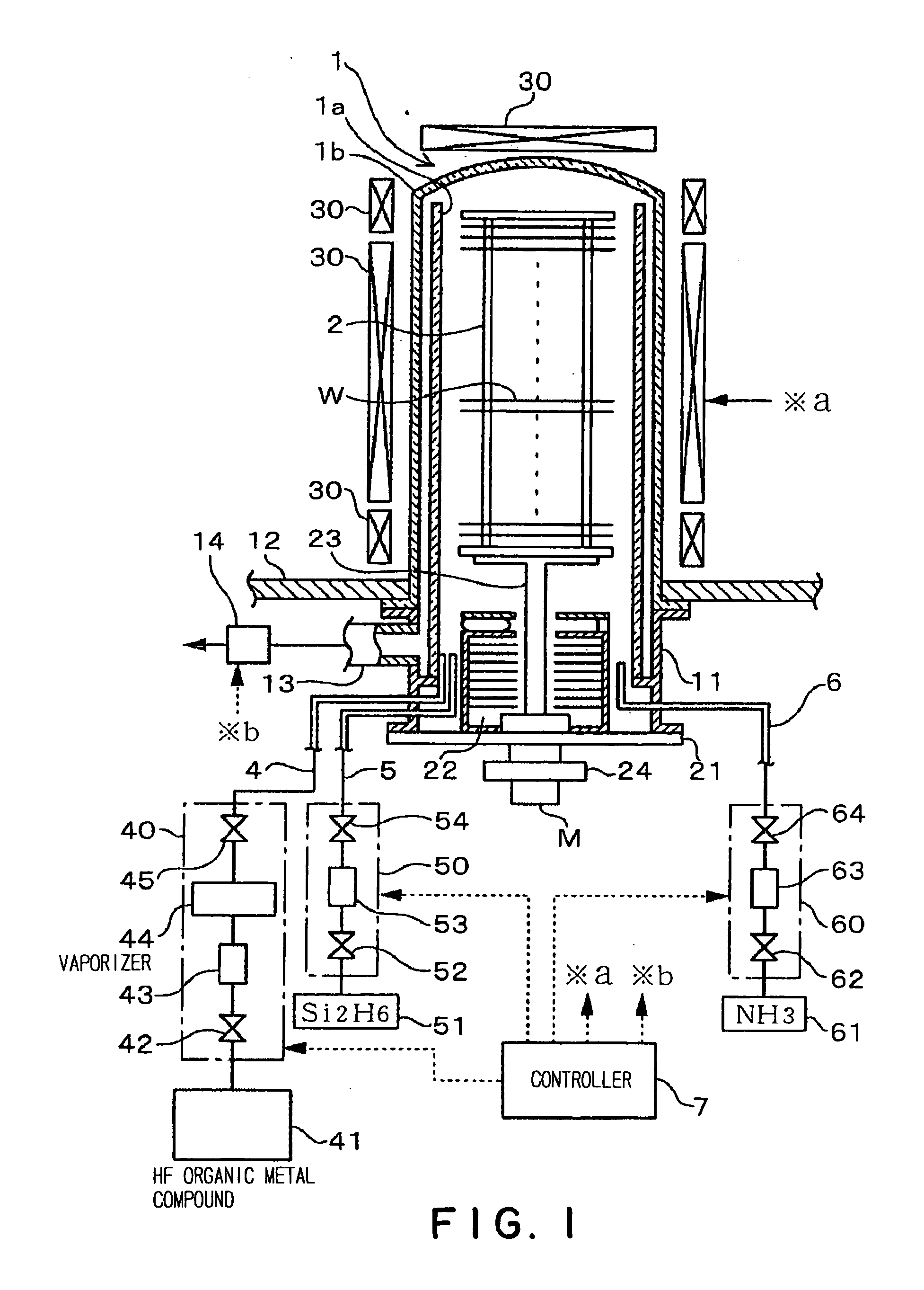
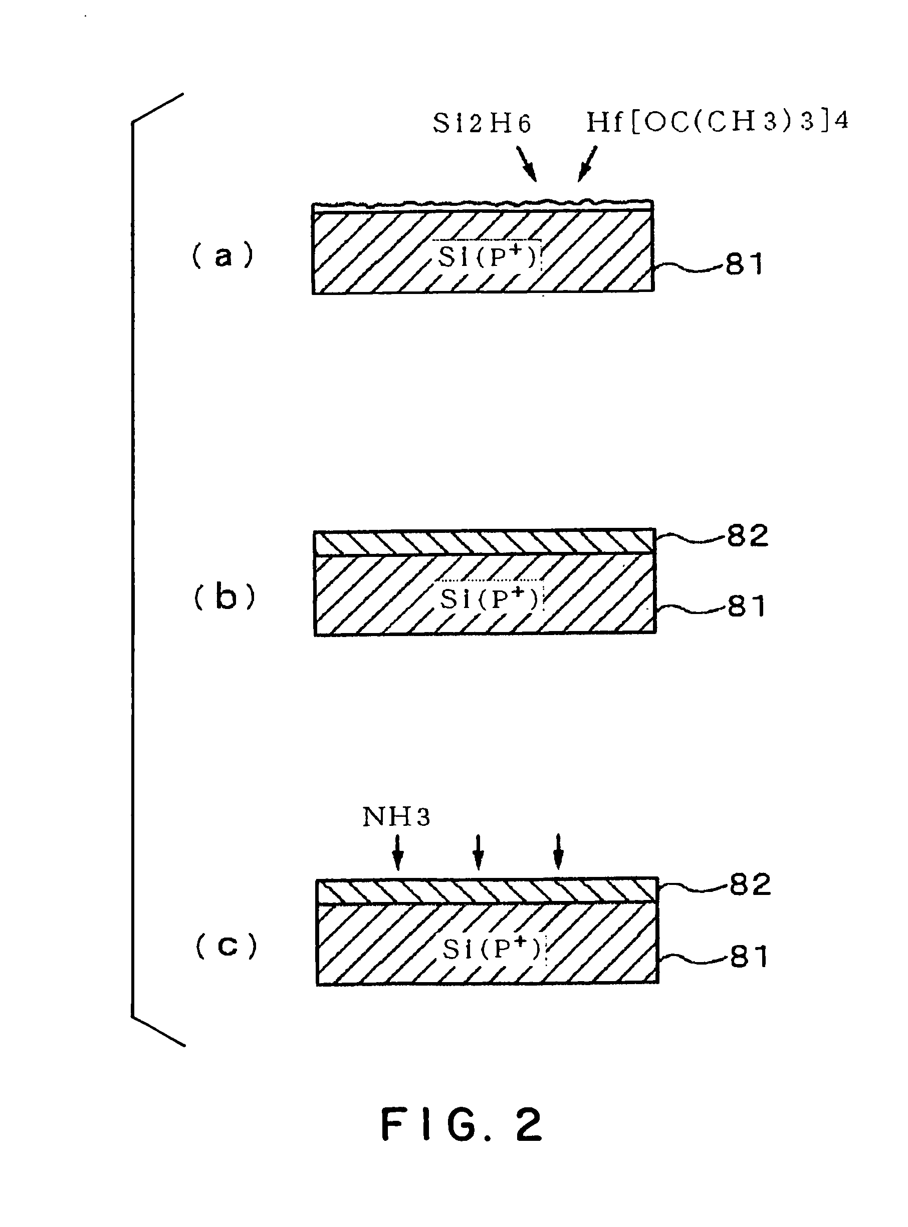
[0052] By using the vertical heat treatment apparatus shown in FIG. 1, hafnium silicate film having a thickness of about 15 nm were deposited on silicon substrates, each having a P-type silicon film previously deposited on a surface thereof. Film-deposition conditions were as follows:

Temperature in the reaction tube: 250° C.

Pressure in the reaction tube: 40 Pa

Flow rate of tetra-tertiary-butoxy hafnium: 0.25 sccm (liquid flow rate)

Flow rate of disilane gas: 1,000 sccm

[0053] In order to examine the crystallization temperature of the hafnium silicate film deposited under the above conditions, the substrates were heated for one minute in an inert gas atmosphere, at different temperatures of 800° C., 850° C., 900° C. and 950° C., respectively. Then, x-ray diffraction analysis was conducted with respect to each of the heated hafnium silicate films. FIG. 4 shows the results. As is apparent from FIG. 4, in the substrate heated at 900° C., a (111) hafnium oxide peak appears at a pos...

example 2

[0054] By using monosilane gas in place of disilane gas, hafnium silicate film having a thickness of about 15 nm were deposited on silicon substrates, each having a P-type silicon film previously deposited on a surface thereof. The flow rate of monosilane gas was 1,000 sccm, which is similar to that of the disilane gas in the Example 1. Other film-deposition conditions were the same as those in Example 1.

[0055] The thus obtained substrates were heated under the same conditions as those in Example 1, and then x-ray diffraction analysis were conducted. FIG. 5 shows the results. As is apparent from FIG. 5, a peak appears in the substrate heated at 850° C., while no peak appears in the substrate heated at 800° C. Thus, it was confirmed that the hafnium silicate film obtained under the film-deposition conditions of Example 2 will not crystallize at 800° C.

[0056] Although the hafnium silicate film deposited by using monosilane gas shows a sufficiently high crystallization temperature, w...

example 3

[0059] Under the same film-deposition conditions as those in Example 1 (a disilane gas was used), hafnium silicate films having a thickness of 12.63 nm were deposited on P-type silicon substrates. Then, the film was subjected to annealing in an ammonia gas atmosphere by using a vertical heat treatment apparatus which was different from the apparatus used for depositing the hafnium silicate films. Annealing conditions were as follows:

Temperature in the reaction tube: 600° C. to 900° C.

Pressure in the reaction tube: 2.66×10² Pa (2 Torr)

Flow rate of ammonia gas: 2 slm

Annealing time: 30 minutes

[0060] The annealed substrates were heated under the same conditions as those in Example 1, and x-ray diffraction analysis was similarly conducted with respect to the films on a surface of each substrate. FIG. 7 shows the results. As is apparent from FIG. 7, a peak appears in the substrate heated at 950° C., while no peak appears in the substrate heated at 900° C. Thus, it was confirmed t...


PUM

PropertyMeasurementUnit
temperatureaaaaaaaaaa
pressureaaaaaaaaaa
pressureaaaaaaaaaa

Abstract

The object of the present invention is to increase the crystallization temperature of a hafnium compound film which can be effectively used as a high dielectric constant film of a gate oxide film of a MOSFET, for example. A hafnium silicate film is deposited on a substrate by reacting a vapor of a hafnium organic compound with a monosilane gas or a disilane gas in a reaction vessel in a heated vacuum atmosphere. Due to the crystallization restraining effect of silicon, the thus obtained film has a higher crystallization temperature. In another embodiment of the present invention, an oxygen-containing hafnium compound film is annealed in a heated ammonia gas atmosphere. The annealing also increase the crystallization temperature of the oxygen-containing hafnium compound film.

Description

FIELD OF THE INVENTION [0001] The present invention relates to a method and an apparatus for forming a high dielectric constant film which can be suitably used as a gate oxide film of a MOSFET (Metal Oxide Semiconductor Field Effect Transistor), a capacitive element of a memory cell, and so on. BACKGROUND ART [0002] A semiconductor device must satisfy various strict requirements. For example, a gate oxide film of a MOSFET must have a small leak current, a large withstand voltage, and high reliability. In addition, there has been recently a demand for reduced capacity to further improve the working speed. By reducing the thickness of the film, the capacity can be reduced. However, when the thickness of a silicon oxide (SiO2) film, which has been conventionally used as a gate oxide film, is reduced, the leak current is undesirably increased to a considerable degree. [0003] Thus, a material having a higher dielectric constant (relative dielectric constant) than that of silicon oxide ha...

Claims


Application Information

Patent Timeline
Patent Type & Authority Applications(United States)
IPC IPC(8): H01L21/31H01L21/469C23C16/40H01L21/316H01L21/8242H01L27/108H01L29/78
CPCC23C16/401H01L21/31645H01L21/02148H01L21/02271H01L21/02211
Inventor NAKAJIMA, SHIGERUCHOI, DONG-KYUNFUJIWARA, TOMONORIIKEGAWA, HIROAKINAKAMURA, GENJI
Owner TOKYO ELECTRON LTD
Why Eureka
Try Eureka