Apparatus and method for laser radiation
a laser radiation and apparatus technology, applied in the field of apparatus, can solve the problems of low efficiency in processing a large area, glass substrate cannot withstand a heating process, laser process,
- Summary
- Abstract
- Description
- Claims
- Application Information
AI Technical Summary
Benefits of technology
Problems solved by technology
Method used
Image
Examples
first embodiment
[0055] the present invention will now be described.
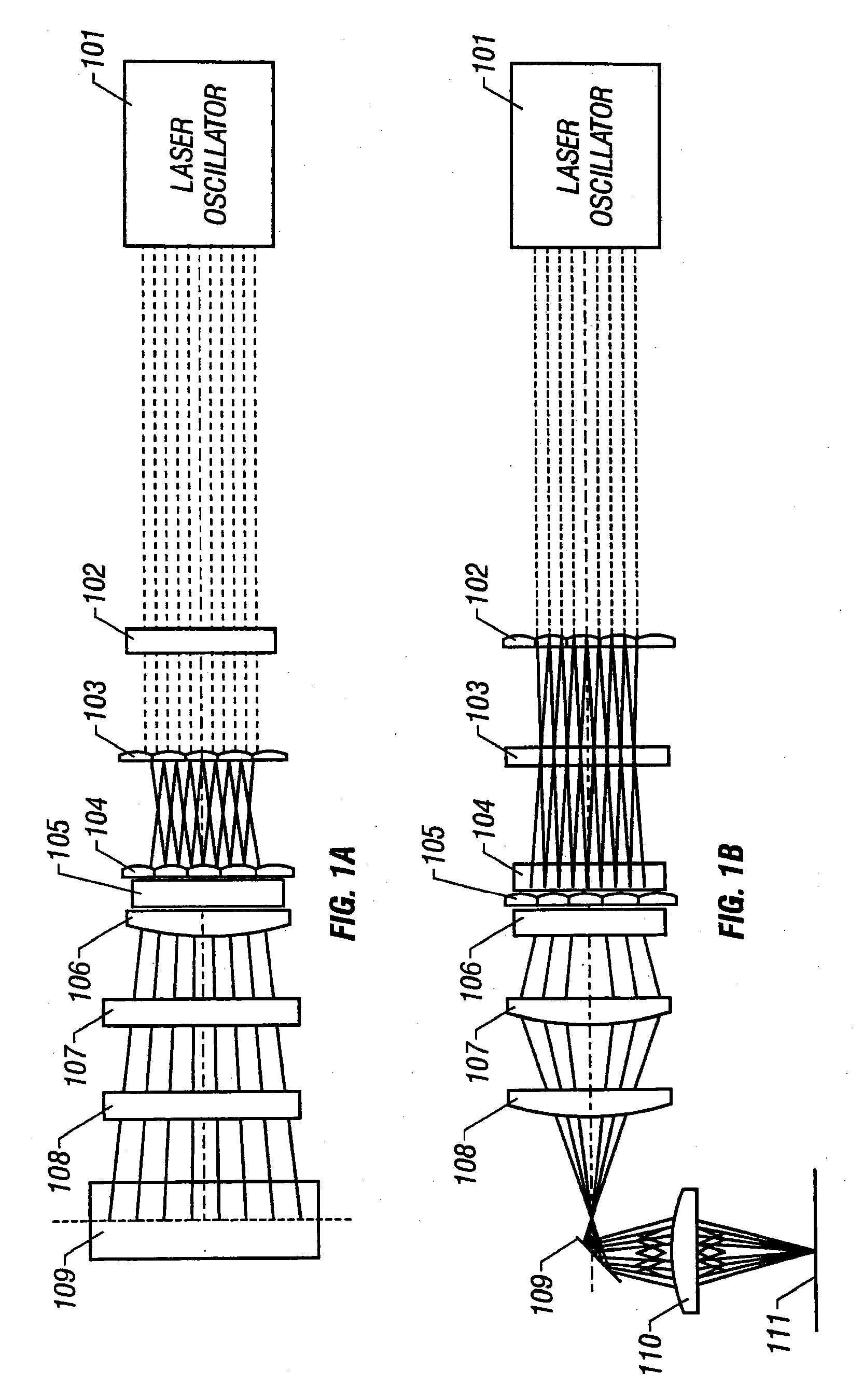
[0056] The present embodiment relates to an optical system in which the number of homogenizers can be one half of that in the optical system shown in FIGS. 1(A) and 1(B).
[0057] FIGS. 6(A) and 6(B) show the optical system of the present embodiment. In the optical system shown in FIGS. 6(A) and 6(B), a laser beam oscillated by an oscillator 601 is shaped by an optical system constituted by lenses 602 and 603 into a laser beam having a predetermined beam shape and predetermined distribution of energy density.
[0058] The distribution of the energy density in this laser beam is corrected by two homogenizers 604 and 605.
[0059] The homogenizer 604 has a function of correcting the energy density of the laser beam which is ultimately shaped into a linear configuration in the direction of the width of the same. However, since the dimension of the linear laser beam in the direction of its width is on the order of a few millimeters, the effec...
second embodiment
[0067] the present invention will now be described.
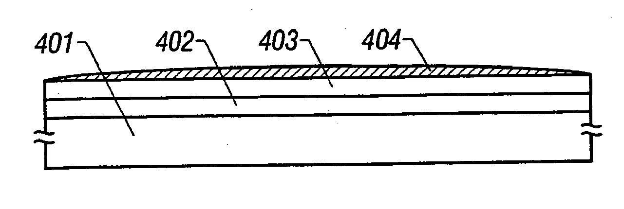
[0068] The present embodiment shows an example of fabrication of a thin film transistor utilizing the present invention. FIGS. 4(A) though 4(F) illustrate steps of fabricating a thin film transistor.
[0069] First, a silicon oxide film or silicon nitride film 402 as a backing layer is formed to a thickness of 3000 Å on a glass substrate indicated by 401 using a sputtering process or plasma CVD process.
[0070] Next, an amorphous silicon film 403 is formed to a thickness of 500 Å using a plasma CVD process or low pressure thermal CVD process. The use of a low pressure thermal CVD process is preferred as a means for forming the amorphous film 403 from the viewpoint of fineness of the film and crystallinity of a crystalline silicon film produced later therefrom.
[0071] In order to improve the effect of annealing using irradiation with a laser beam, it is important that the thickness of the amorphous film 403 is 1000 Å or less and more pr...
third embodiment
[0103] the present invention will now be described.
[0104] The present embodiment is an example wherein an XeCl laser (having a wavelength of 308 nm) is used in the configuration as described in the second embodiment.
[0105] The use of a KrF excimer laser having a short wavelength (248 nm) is preferred from the viewpoint of the annealing effect on the silicon film. This is because a laser beam having a shorter wavelength is more easily absorbed by the silicon film.
[0106] However, when the maintenance of the apparatus and the stability of the oscillator is taken into consideration, it is preferable to use an XeCl excimer laser having a wavelength longer than that of a KrF excimer laser.
[0107] The reason is that a longer wavelength means lower photon energy (hν) and a lighter load to the optical system and oscillator.
PUM
| Property | Measurement | Unit |
|---|---|---|
| length | aaaaa | aaaaa |
| length | aaaaa | aaaaa |
| temperatures | aaaaa | aaaaa |
Abstract
Description
Claims
Application Information


