Polarization-doped field effect transistors (POLFETS) and materials and methods for making the same

a field effect transistor and polarization-induced doping technology, which is applied in the direction of transistors, electrical devices, semiconductor devices, etc., can solve the problems of limiting the choice of g/sub>m/sub>-v/sub>gs /sub>profiles, and the structure of traditional algan/gan hemt-like devices does not lead to easy modification of g/sub>m/sub>-v/sub>

Inactive Publication Date: 2006-10-19
RGT UNIV OF CALIFORNIA
View PDF6 Cites 30 Cited by
  • Summary
  • Abstract
  • Description
  • Claims
  • Application Information

AI Technical Summary

Benefits of technology

[0011] According to one aspect of the present invention, a III-V Nitride based heterostructure is provided that typically includes a polarization doped III-V Nitride composition. In certain aspects, the composition comprises a compositionally graded Nitride layer where compositional grading is done between any two Nitride based alloys such that the resulting polarization creates a conducting channel, e.g., either an n-type or a p-type conducting channel. For example, in one aspect, the composition includes AlxGa1−xN graded over a distance to AlyGa1−yN, where x and y are different and where x and y are each selected from a range from about 0 to 1.0, and where the grading distance may range from about 1.0 nm to about 1,000 nm or more. In one aspect, x is 0 and y is about 0.3. In another aspect, compositional grading may be done using InGaN-based alloys in Ga-polar orientation or in N-polar orientation. In another aspect, compositional grading may be done using AlInGaN-based alloys in Ga-polar orientation or in N-polar orientation. The grading function may be a linear function, a parabolic function or other function. In certain aspects, the compositional grading function is selected to specifically change or improve the transconductance profile, microwave linearity and / or other properties of the composition.

Problems solved by technology

However, the structure of traditional AlGaN / GaN HEMT-like devices does not lead itself to easy modification of the gm-Vgs profile.
However, the device designer is constrained in their choice of channel charge due to gate leakage, breakdown and impurity scattering limited mobility.

Method used


Image

  • Polarization-doped field effect transistors (POLFETS) and materials and methods for making the same
  • Polarization-doped field effect transistors (POLFETS) and materials and methods for making the same
  • Polarization-doped field effect transistors (POLFETS) and materials and methods for making the same

Examples


Embodiment Construction

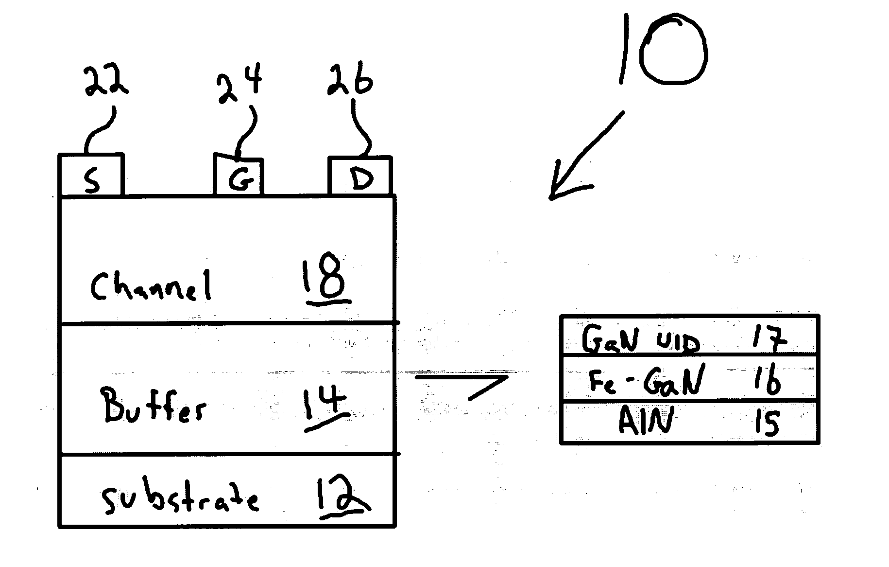
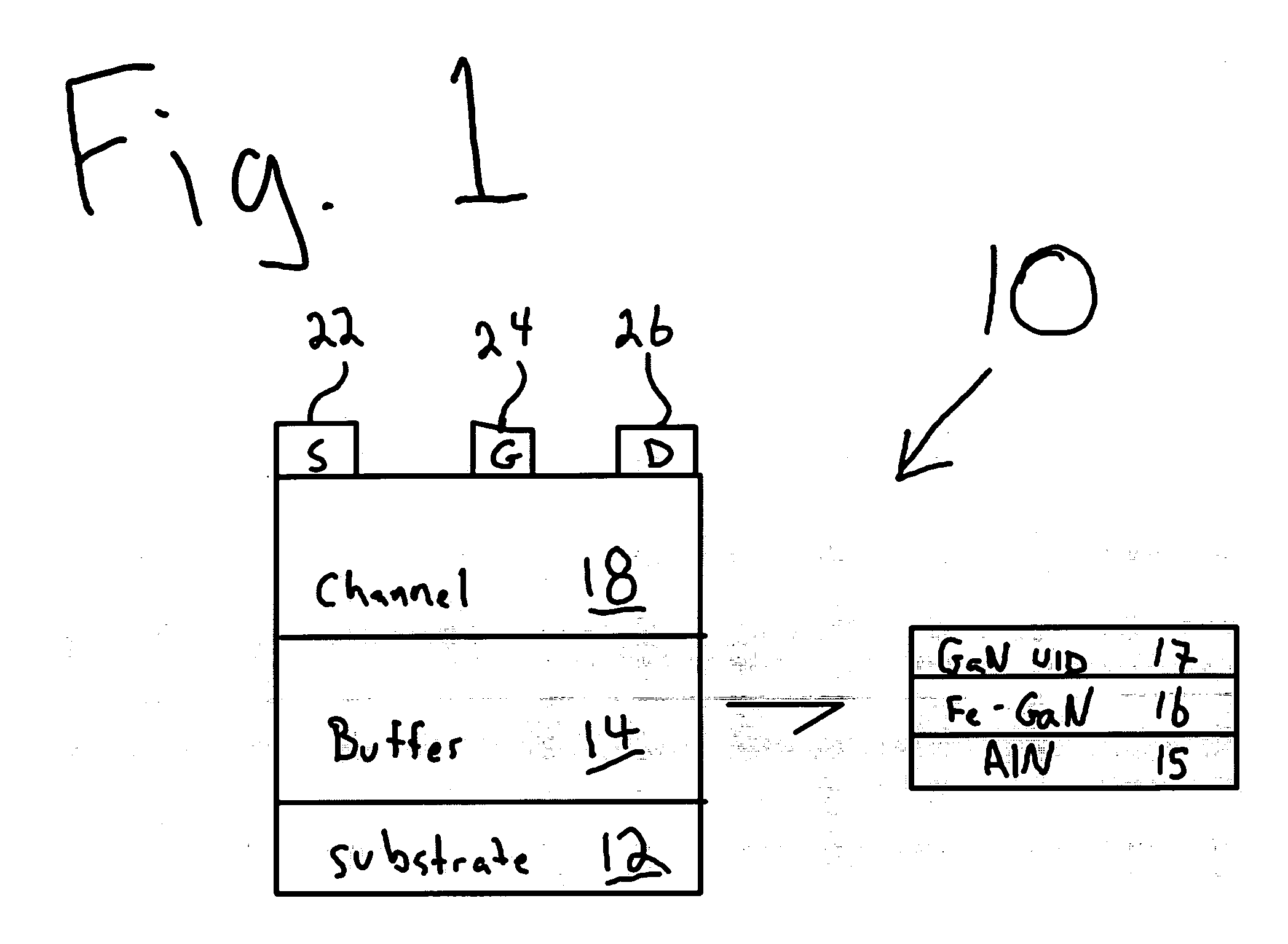
[0019] The present invention provides improved materials and devices for use in microwave power and other applications. In one aspect, improved device performance results from the superior carrier transport properties achieved by polarization-induced bulk electron doping, compared with impurity-doped carriers, which are highly desirable for electronic devices. Junction field effect transistors (JFETs) and metal-semiconductor field effect transistors (MESFETs), and other devices can be made in III-V Nitride material systems using the techniques and teachings of the present invention. In one aspect, in devices according to the present invention, an electron channel is formed by grading across a heterojunction, such as an AlGaN / GaN heterojunction, over a distance. For example, in certain aspects, device templates may be created by grading linearly from AlxGa1−xN to AlyGa1−yN on (0001) semi-insulating GaN, where x and y are typically different and where x may range from 0 (GaN) to 1.0 a...


PUM


Abstract

Novel GaN / AlGaN metal-semiconductor field-effect transistor (MESFET) structures grown without any impurity doping in the channel. A high-mobility polarization-induced bulk channel charge is created by grading the channel region linearly from GaN to Al0.3Ga0.7N over a distance, e.g., 1000 Å. A polarization-doped field effect transistor (PolFET) was fabricated and tested under DC and RF conditions. A current density of 850 mA / mm and transconductance of 93 mS / mm was observed under DC conditions. Small-signal characterization of 0.7 μm gate length devices had a cutoff frequency, ƒτ=19 GHz, and a maximum oscillation of ƒmax=46 GHz. The PolFETs perform better than comparable MESFETs with impurity-doped channels, and are suitable for high microwave power applications. An important advantage of these devices over AlGaN / GaN HEMTs is that the transconductance vs. gate voltage profile can be tailored by compositional grading for better large-signal linearity.

Description

CROSS-REFERENCES TO RELATED APPLICATIONS [0001] This application claims the benefit of U.S. Provisional Application 60 / 614,585, filed Sep. 29, 2004, titled “Polarization-Doped Field Effect Transistor (POLFETS) and Materials and Methods for Making the Same” which is hereby incorporated by reference in its entirety.STATEMENT AS TO RIGHTS TO INVENTIONS MADE UNDER FEDERALLY SPONSORED RESEARCH AND DEVELOPMENT [0002] The government may have certain rights to the invention based in ONR / CANE MURI Grant Number N00014-01-1-0764 and ONR / POLARIS MURI Grant Number N00014-99-1-0829.BACKGROUND OF THE INVENTION [0003] The present invention relates generally to materials for use in transistors, and more particularly to polarization-induced bulk doping in electronic materials exhibiting strong spontaneous and / or piezoelectric polarization (e.g., ferroelectric and / or piezoelectric materials), and the use of these materials in forming high electron mobility field-effect transistor devices. [0004] Prior...

Claims


Application Information

Patent Timeline
Patent Type & Authority Applications(United States)
IPC IPC(8): H01L31/00
CPCH01L29/1029H01L29/2003H01L29/812H01L29/7787H01L29/7783
Inventor MISHRA, UMESH K.XING, HUILIJENA, DEBDEEPRAJAN, SIDDHARTH
Owner RGT UNIV OF CALIFORNIA
Why Eureka
Try Eureka