Main board for backplane buses

a backplane bus and main board technology, applied in the direction of orthogonal pcbs mounting, cross-talk/noise/interference reduction, high frequency circuit adaptation, etc., can solve the problem of more significant signal attenuation, electrical restrictions on printed circuit boards, signal waveform disturbance, etc., to suppress crosstalk noise and power supply noise, the effect of reducing nois

Inactive Publication Date: 2006-10-19
HITACHI LTD
View PDF5 Cites 26 Cited by
  • Summary
  • Abstract
  • Description
  • Claims
  • Application Information

AI Technical Summary

Benefits of technology

[0036] Constructing the motherboard in this way makes it possible for the noise propagated between the power supply layers with respect to a desired signal to be reduced in a specific frequency band (3-5 GHz) while the EBG pattern is maintaining a direct current. More particularly, such construction is contributive to suppressing the crosstalk noise and power supply noise generated by the signals asynchronously transmitted between other modules.
[0037] According to the pr

Problems solved by technology

One of the problems encountered in transmitting digital signals of a 10-Gbps (gigabits per second) class is that the signal waveforms become disturbed.
This problem arises from electrical restrictions on the printed-circuit board that constitutes wiring.
That is to say, the above is because metallic wiring attenuates signals by a skin effect more significantly at higher frequencies and because the dielectric losses in insulators also cause more significant signal attenuation at higher frequencies.
These factors have frequency dependence and cause more significant attenuation at higher frequencies.
In this context, the noise occurring on the circuit boards of electronic devices is a big problem.
However, if the power supply layer and the ground layer are arranged in opposed form as in a motherboard for backplane buses, the consequent composition of a resonator between the two layers presents the problem that power supply noise superimposition on signals occurs at a resonance frequency.
The superimpositi

Method used


Image

  • Main board for backplane buses
  • Main board for backplane buses
  • Main board for backplane buses

Examples


first embodiment

[0061] A first embodiment of the present invention is described below with reference to FIGS. 1 to 9.

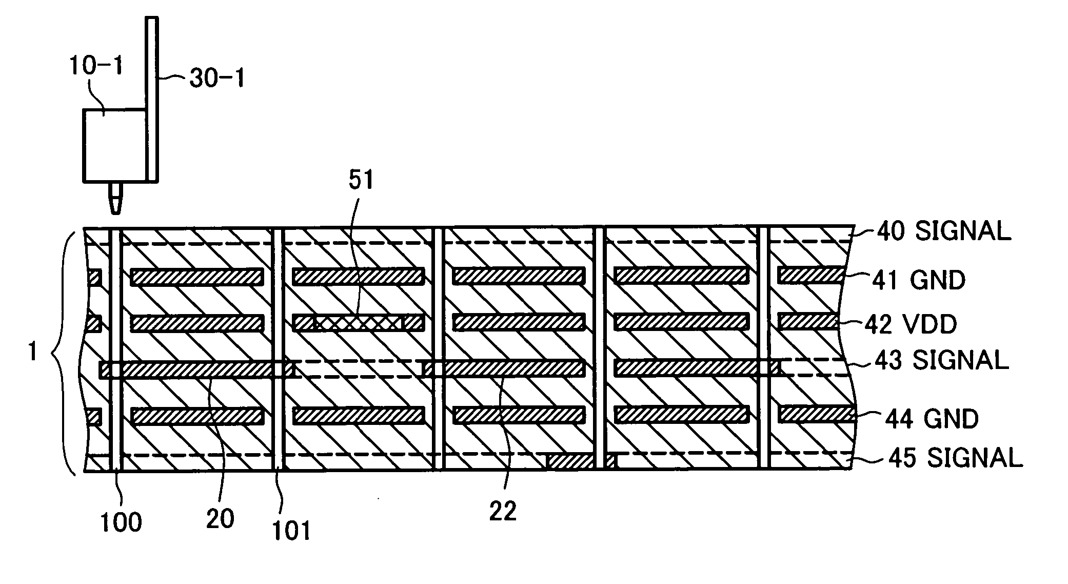
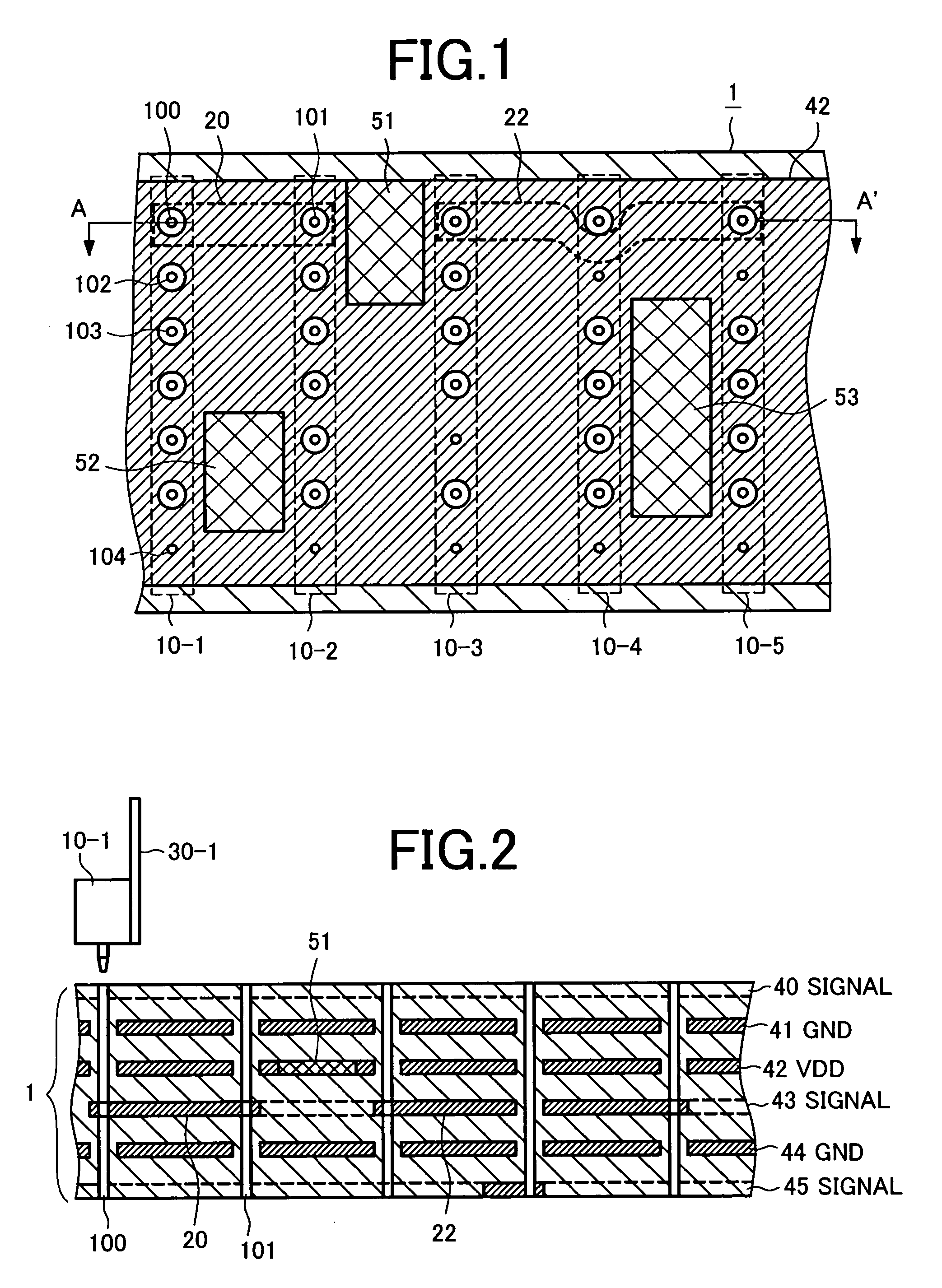
[0062]FIG. 1 is a horizontal cross-sectional view of a motherboard for backplane buses according to the first embodiment of the present invention, showing a section extending along a power supply layer 42 (see FIG. 2).

[0063]FIG. 2 is a vertical cross-sectional view that shows section A-A′ of the above motherboard for backplane buses.

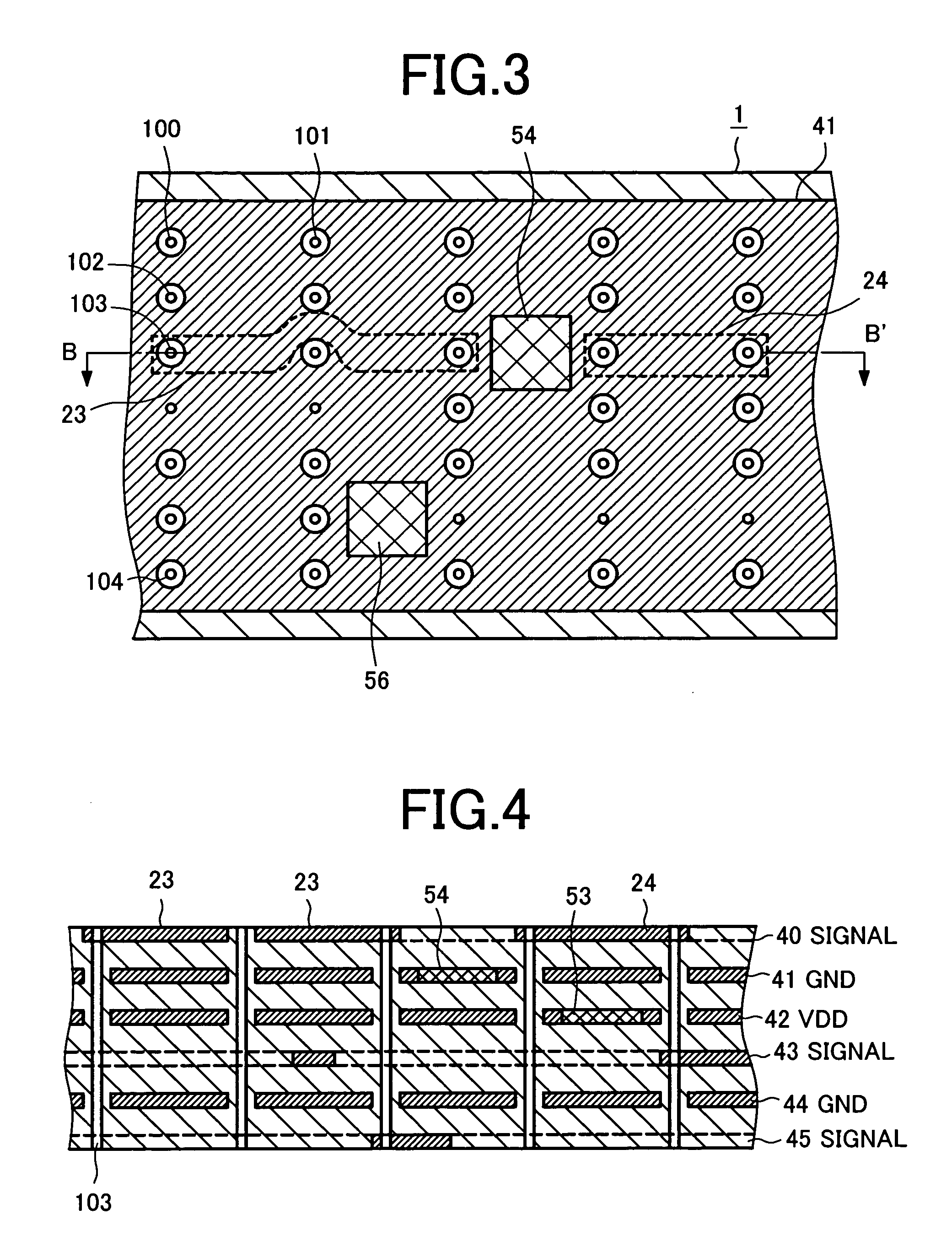
[0064]FIG. 3 is a horizontal cross-sectional view of the above motherboard for backplane buses, showing a section extending along a ground layer 41.

[0065]FIG. 4 is a vertical cross-sectional view that shows section B-B′ of the above motherboard for backplane buses.

[0066] Motherboard 1 is a multilayer wiring board, including a first signal layer 40 that connects connector wiring, a first ground layer 41, a power supply layer (VDD) 42, a second signal layer 43, a second ground (GND) layer 44, and a third signal layer 45. These layers are each stacked v...

second embodiment

[0086] A second embodiment according to the present invention will be described hereunder with reference to FIGS. 10, 11.

[0087]FIG. 10 is a vertical cross-sectional view of a motherboard for backplane buses according to the second embodiment, showing a section extending along an array of via holes.

[0088] In the present embodiment, a signal layer 43′ is added to the layer configuration shown in FIG. 2. The present embodiment is exactly the same as the first embodiment of FIGS. 1 to 4, except that a power supply layer 42 is formed as an EBG pattern only in an associated region 51 between independent electrical lines 20, 22 of a second signal layer 43. The region 51 is also a region present between independent wiring patterns 20′ and 22′ of the added signal layer 43′. The EBG pattern of the region 51, therefore, is also effective for cutting offnoise between the electrical lines 20′, 22′ of the added signal layer 43′.

[0089] Noise between independent signal nodes can be cut off simil...

third embodiment

[0091] A third embodiment according to the present invention will be described hereunder with reference to FIGS. 12, 13.

[0092]FIG. 12 is a horizontal cross-sectional view showing in part a power supply layer 42 of a motherboard for backplane buses according to the third embodiment.

[0093]FIG. 13 is a vertical cross-sectional view of section C-C′ of the above motherboard.

[0094] In addition to EBG patterns similar to those described in FIGS. 1, 2, the power supply layer 42 in the motherboard of the present embodiment has EBG patterns 51b, 52b, 53b, 54b, 55b, each of these patterns extending in a horizontal direction of FIG. 12. A majority of wiring patterns formed on the signal layer 43 extend horizontally to interconnect the pins located at the same positions in different connectors, and these patterns resemble, for example, wiring patterns 20, 21 of FIG. 12. The EBG patterns 51b, 52b, 53b, 54b, 55b are effective for cutting off the noise propagated between the above wiring pattern...


PUM


Abstract

A motherboard for backplane buses is provided that reduces noise due to entry of external signals into signal wiring which interconnects modules, or noise due to any external signals entering a power supply after being routed around the power supply. An EBG pattern formed up of two wiring regions different from each other in impedance is periodically disposed in at least three arrays as part of the power supply layer(s) constituting a microstripline structure (one layer adjacent to a signal layer is a power supply layer, and the other layer-is interposed in air) or a stripline structure (both layers adjacent to a signal layer are power supply layers); the part of the power supply layer(s) not being involved in signal transmission between the modules on the motherboard for backplane buses.

Description

CLAIM OF PRIORITY [0001] The present application claims priority from Japanese application JP 2005-119304, filed on Apr. 18, 2005, the content of which is hereby incorporated by reference into this application. BACKGROUND OF THE INVENTION [0002] 1. Field of the Invention [0003] The present invention relates generally to main boards for backplane buses. The invention also relates to a bus connection technique used for personal computers, servers, routers, and other information-processing units in order to interconnect functional circuits such as a processor and a memory. More particularly, the invention relates to a main board for backplane buses, suitable for reducing radio-frequency noise. [0004] 2. Description of the Related Art [0005] One of the problems encountered in transmitting digital signals of a 10-Gbps (gigabits per second) class is that the signal waveforms become disturbed. This problem arises from electrical restrictions on the printed-circuit board that constitutes wi...

Claims


Application Information

Patent Timeline
IPC IPC(8): H05K7/06
CPCH05K1/0236H05K1/0237H05K1/0298H05K2201/0969H05K2201/044H05K2201/09681H05K1/167
Inventor OSAKA, HIDEKI
Owner HITACHI LTD
Why Eureka
Try Eureka