Split gate flash memory cell and manufacturing method thereof

a technology of flash memory cell and split gate, which is applied in the direction of semiconductor devices, basic electric elements, electrical equipment, etc., can solve the problems of erroneous data interpretation, difficult control of the amount of electron discharge, and negative charge leaving the floating gate, so as to increase the gate coupling ratio and the effect of device integration

Active Publication Date: 2006-10-19
POWERCHIP SEMICON MFG CORP
View PDF6 Cites 19 Cited by
  • Summary
  • Abstract
  • Description
  • Claims
  • Application Information

AI Technical Summary

Benefits of technology

[0010] Accordingly, the present invention provides a split gate flash memory cell and a manufacturing method thereof, wherein the gate coupling ratio and the integration of devices can be increased.

Problems solved by technology

During the erasure of information of the above flash memory device, the amount of electrons being discharged is difficult to control.
Consequently, over-erase is resulted when an excessive amount of the electrons are discharged from the floating gate, leaving the floating gate with positive charges.
When the over-erase phenomenon is serious, a channel current flow is induced under the floating gate even no working voltage is applied to the control gate, leading to an erroneous interpretation of the data.
As a result, the gate coupling ratio and the integration of devices can not be increased.

Method used


Image

  • Split gate flash memory cell and manufacturing method thereof
  • Split gate flash memory cell and manufacturing method thereof
  • Split gate flash memory cell and manufacturing method thereof

Examples


Embodiment Construction

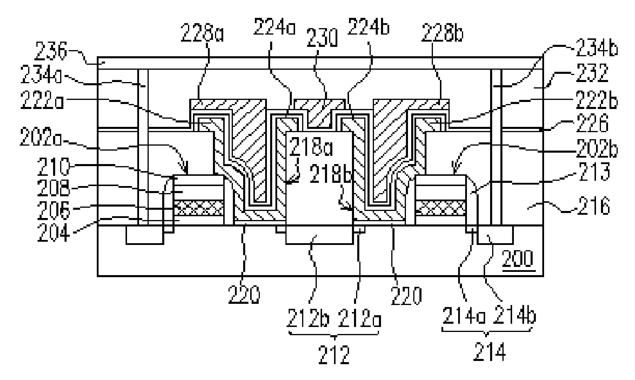
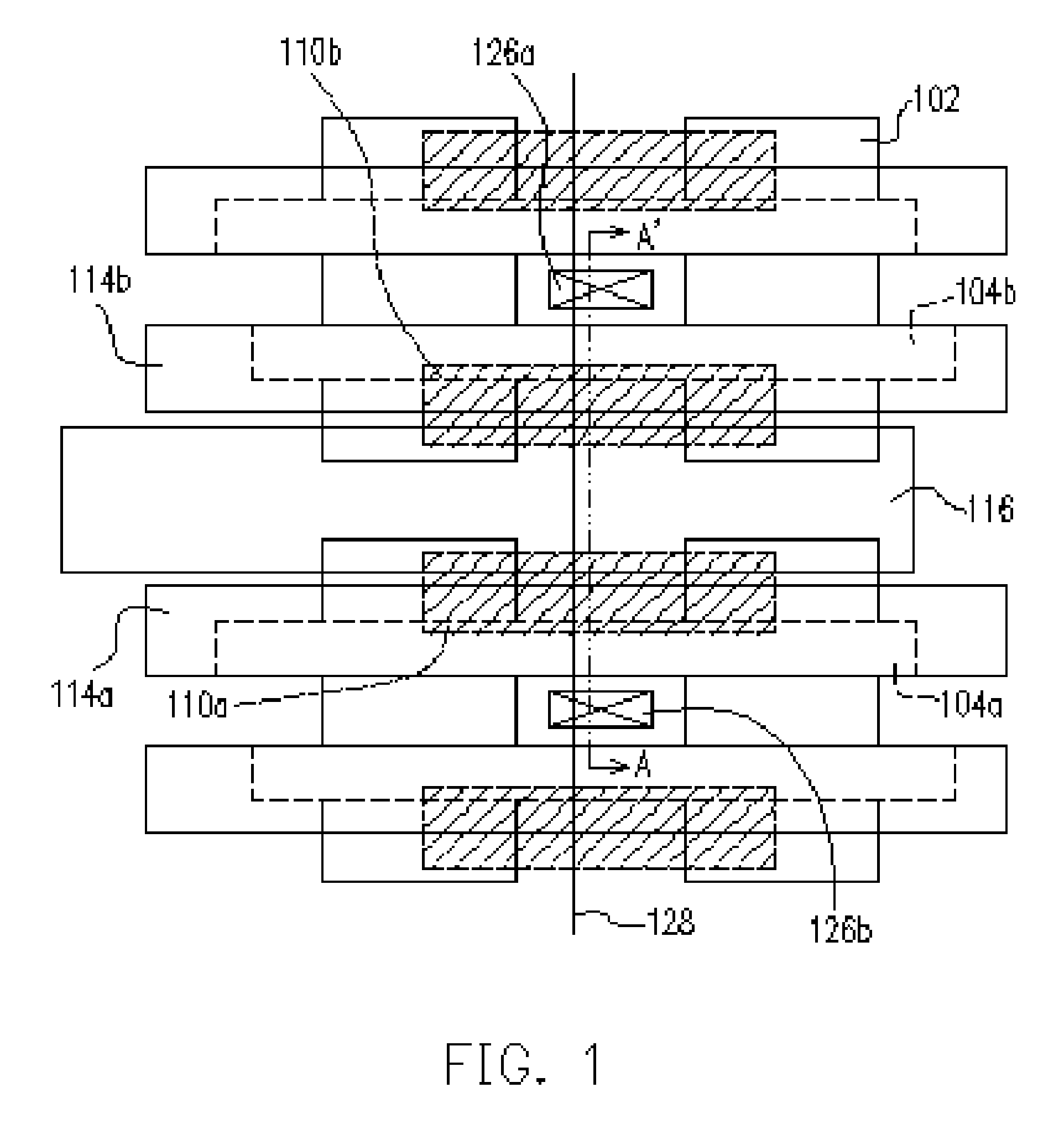
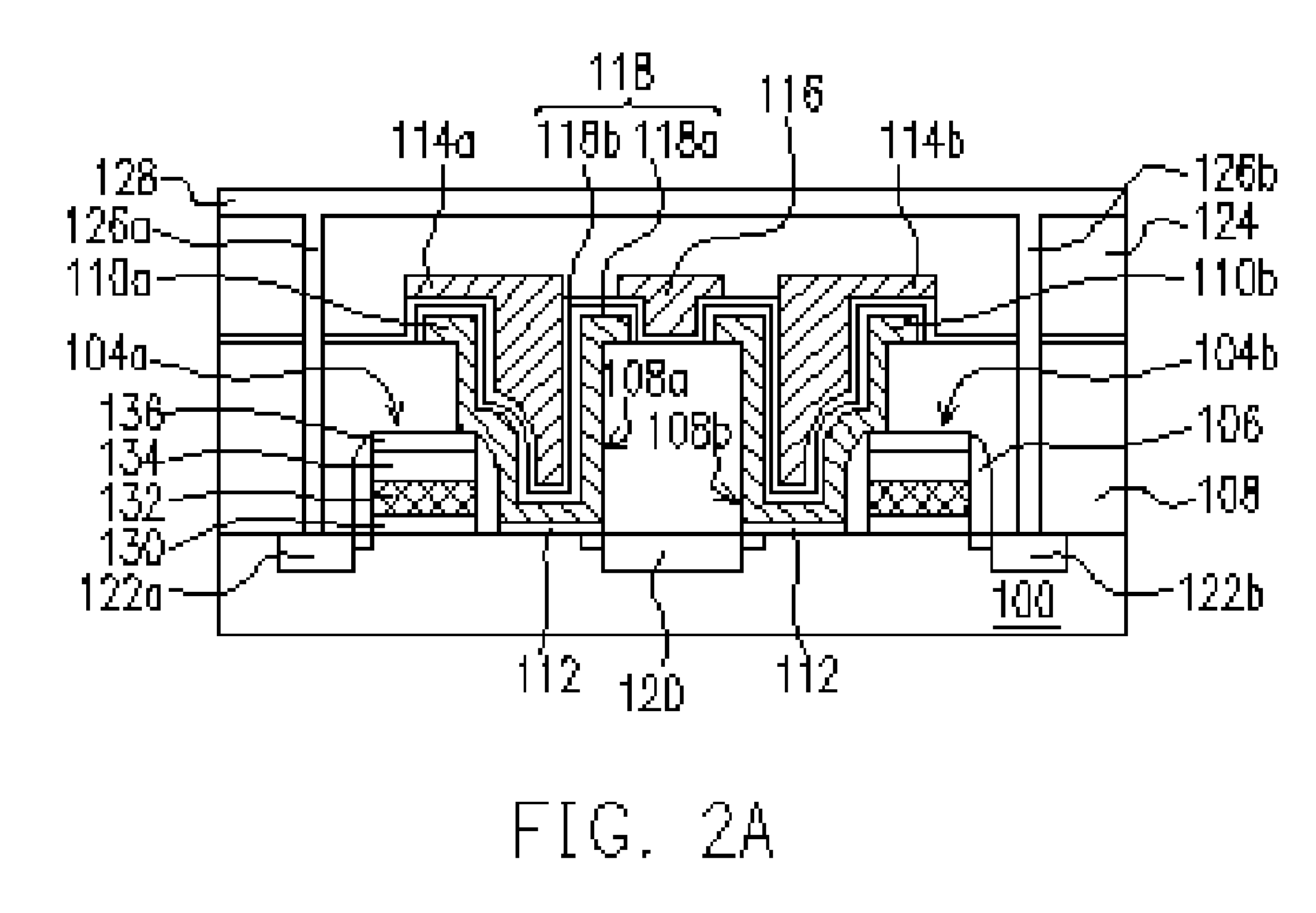
[0028]FIG. 1 is a schematic, top view diagram illustrating a structure of a split gate flash memory cell according to the present invention. FIG. 2A is a schematic, cross-sectional view diagram of a split gate flash memory cell according to one aspect of the present invention. FIG. 2A is a cross-sectional view diagram of FIG. 1 along the cutting line A-A. FIG. 2B is a schematic, cross-sectional view diagram of a split gate flash memory cell according to another aspect of the present invention. In FIGS. 1, 2A and 2B, the same reference numbers are used in the drawings to refer to the same or like parts.

[0029] Referring to both FIGS. 1 and 2A, the flash memory cell of the present invention is formed with a substrate 100, a device isolation structure 102, an inter-layer dielectric layer 108, a floating gate 110a and a floating gate 110b, a tunneling dielectric layer 112, a control gate 114a and a control gate 114b, an erase gate 116, a gate dielectric layer 118, a source region 120, a...


PUM


Abstract

A split gate flash memory cell includes a substrate having a device isolation structure; a selective gate structure disposed on the substrate; an interlayer dielectric layer having an opening disposed on the substrate, wherein the opening exposes a portion of the selective gate structure, the substrate and the device isolation structure; a floating gate disposed in the opening and extended to cover a surface of the interlayer dielectric layer; a tunneling dielectric layer disposed between the floating gate and the selective gate structure; a gate dielectric layer disposed between the floating gate and the control gate; a source region disposed in the substrate on one side of the control gate that is not adjacent to the selective gate structure, and a drain region disposed in the substrate on one side of the selective gate that is not adjacent to the control gate.

Description

CROSS-REFERENCE TO RELATED APPLICATION [0001] This application is a divisional of a prior application Ser. No. 10 / 605,198, filed Sep. 15, 2003, now pending.BACKGROUND OF THE INVENTION [0002] 1. Field of the Invention [0003] The present invention relates to a semiconductor device. More particularly, the present invention relates to a split gate flash memory cell and a manufacturing method thereof. [0004] 2. Description of Related Art [0005] A flash memory device provides the property of multiple entries, retrievals and erasures of data. Moreover, the stored information is retained even electrical power is interrupted. As a result, a non-volatile memory device is widely used in personal computers and electronic systems. [0006] A typical flash memory device employs doped polysilicon to fabricate the floating gate and the control gate. Further, a dielectric layer is used to isolate the floating gate from the control gate, while the floating gate and the substrate are isolated from each ...

Claims


Application Information

Patent Timeline
Patent Type & Authority Applications(United States)
IPC IPC(8): H01L21/336
CPCH01L27/115H01L27/11524H01L27/11521H01L27/11519H10B41/10H10B69/00H10B41/30H10B41/35
Inventor WU, SHENGHUANG, TSAI-YU
Owner POWERCHIP SEMICON MFG CORP
Why Eureka
Try Eureka