Solid state imaging device

a solid-state imaging and imaging device technology, applied in the field of solid-state imaging devices, can solve the problems of deterioration of transistor characteristics, new facilities and new processes, and increased costs, and achieve the effect of increasing the ratio of device regions and high packing density

Inactive Publication Date: 2006-10-26
COLLABO INNOVATIONS INC
View PDF6 Cites 9 Cited by
  • Summary
  • Abstract
  • Description
  • Claims
  • Application Information

AI Technical Summary

Benefits of technology

[0018] In order to solve the above-described conventional problems, the present invention intends to increase the ratio of the device region in which the pixels are formed to the chip area without hindering the entrance of light into the pixels, thereby achieving a solid state imaging device with high packing density.
[0021] According to the solid state imaging device of the present invention, a region for forming the pads for external connection and a region for interconnection are integrated. As a result, the ratio of the device region to the solid state imaging device increases. Further, since the region for forming the pads is completely separated from a region for forming the pixels, the pads will not hinder the entrance of light into the pixels.
[0022] As to the solid state imaging device of the present invention, the pads are preferably located above the horizontal transfer channel. According to the structure, the ratio of the area occupied by the pads is reduced to a further degree and the pads function as a light shield film. Therefore, the efficiency of horizontal charge transfer improves.
[0024] As to the solid state imaging device of the present invention, the pads are preferably inclined from the main surface of the semiconductor chip. According to the structure, a mounting angle at which bonding wires are connected to the pads is reduced, thereby preventing the bonding wires from blocking the light incident on the pixels.
[0025] As to the solid state imaging device of the present invention, the pads are preferably electrically connected to the bus interconnects via contact plugs. According to the structure, the connection between the pads and the bus interconnects is simplified, thereby reducing the chip size to a further degree.

Problems solved by technology

However, the miniaturization of the impurity diffusion regions and the interconnects leads to deterioration in characteristic of the transistor.
In addition, new facilities and new processes must be introduced and the cost increases.
As a result, the sensitivity and the saturation characteristic which are important for the solid state imaging device deteriorate.

Method used


Image

  • Solid state imaging device
  • Solid state imaging device
  • Solid state imaging device

Examples


first embodiment

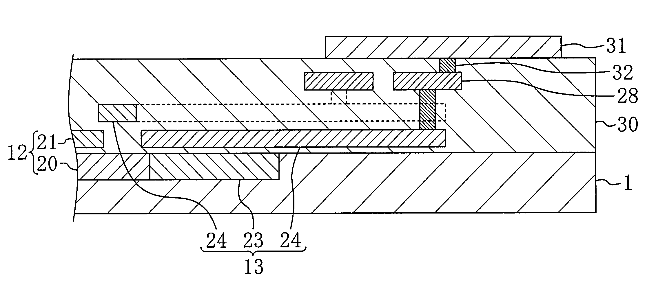
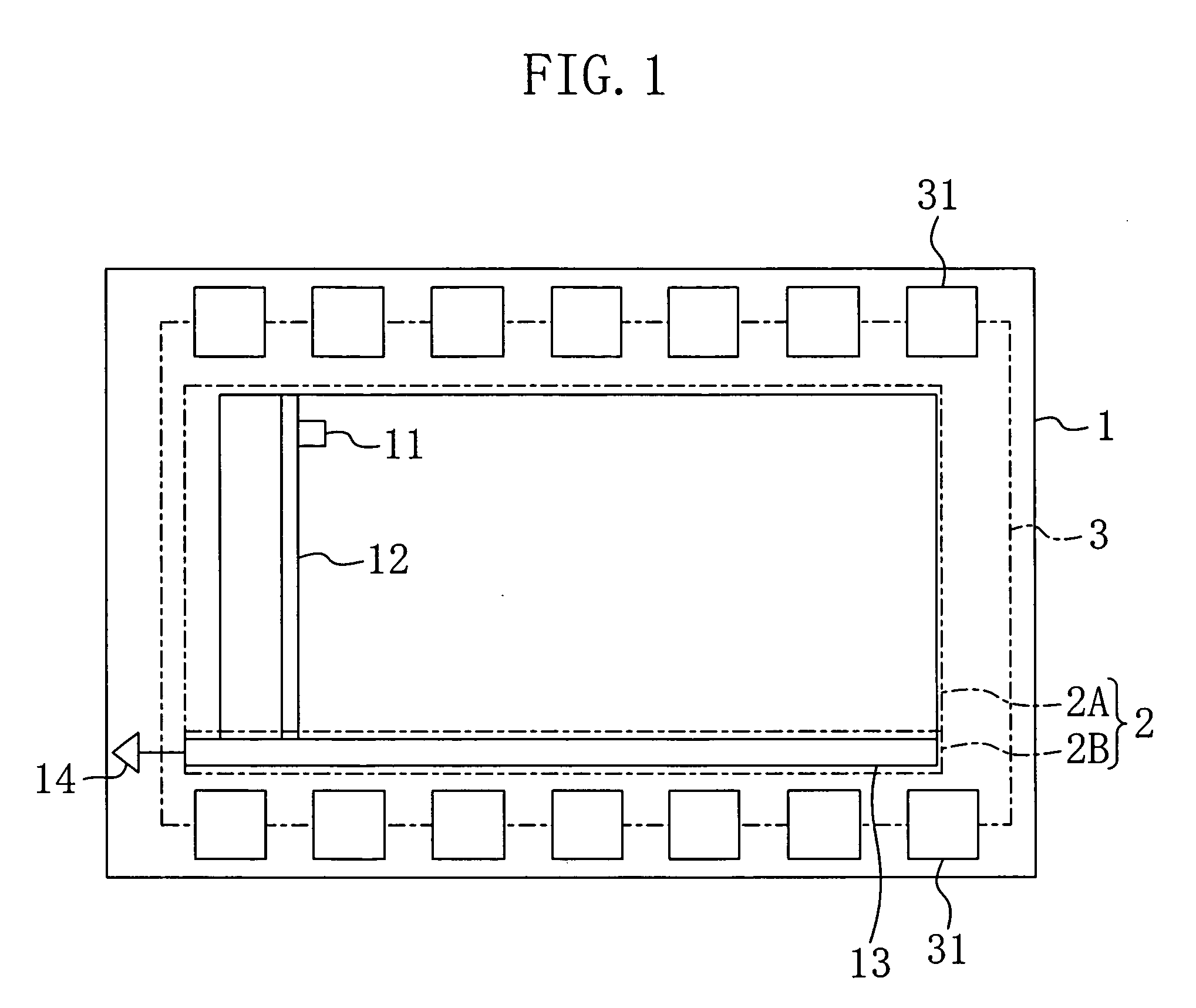
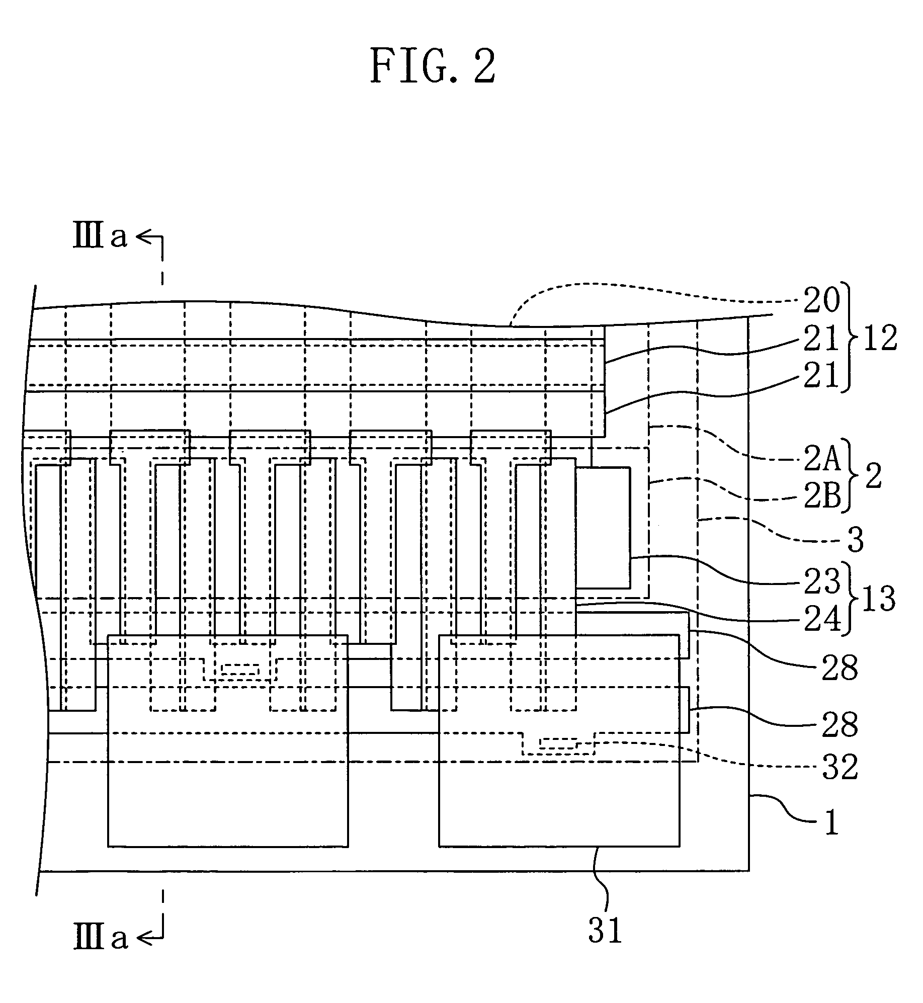
[0038] With reference to the drawings, an explanation of a solid state imaging device of the first embodiment of the present invention will be provided. FIGS. 1 to 3 show the solid state imaging device of the first embodiment. Specifically, FIG. 1 shows a plane structure, FIG. 2 is an enlargement of FIG. 1 and FIG. 3 shows a section taken along the line IIIa-IIIa of FIG. 2.

[0039] As shown in FIGS. 1 to 3, a plurality of pixels 11 are arranged in a matrix in a pixel region 2A of a semiconductor chip 1. The pixels 11 are photodiodes and generate signal charge corresponding to the intensity of light incident thereon.

[0040] Vertical transfer registers 12 extending in the column direction are arranged between the pixels 11 adjacent to each other. Each of the vertical transfer registers 12 includes a vertical transfer channel 20 which is an impurity diffusion layer formed in the surface of the semiconductor chip 1 and extends in the column direction and a plurality of vertical transfer ...

second embodiment

[0056] Hereinafter, an explanation of a solid state imaging device according to a second embodiment of the present invention will be provided with reference to the drawings. FIGS. 4 to 6 show the solid state imaging device according to the second embodiment. Specifically, FIG. 4 shows a plane structure, FIG. 5 is an enlargement of FIG. 4 and FIG. 6 shows a section taken along the line VIa-VIa of FIG. 5. In FIGS. 4 to 6, the same components as those shown in FIGS. 1 to 3 are indicated by the same reference numerals to omit the explanation.

[0057] In the solid state imaging device of the present embodiment, the pads 31 for external connection are formed to overlap with the interconnect region 3 and the horizontal transfer register region 2B. Specifically, part of each pad 31 is located above the horizontal transfer channel 23.

[0058] The metal layer for forming the pads 31 made of aluminum, copper, gold or platinum surely blocks light as compared with the conductive layer for forming ...

third embodiment

[0060] Hereinafter, an explanation of a solid state imaging device according to a third embodiment of the present invention will be provided with reference to the drawings. FIGS. 7 to 9 show the solid state imaging device according to the third embodiment. Specifically, FIG. 7 shows a plane structure, FIG. 8 is an enlargement of FIG. 7 and FIG. 9 shows a section taken along the line IXa-IXa of FIG. 8. In FIGS. 7 to 9, the same components as those shown in FIGS. 1 to 3 are indicated by the same reference numerals to omit the explanation.

[0061] In the solid state imaging device of the present embodiment, part of the interlayer insulating film 30 in the interconnect region 3 is gradually reduced in thickness toward the periphery of the chip to have an inclined surface and the pads 31 for external connection are formed on the inclined surface.

[0062] In order to obtain the inclined surface, a resist mask is formed to cover other part of the interlayer insulating film 30 than the part f...


PUM


Abstract

A solid state imaging device includes: a plurality of photoelectric conversion elements which are arranged in a two-dimensional matrix on a semiconductor chip; vertical transfer registers including a vertical transfer channel and vertical transfer electrodes, respectively, for transferring signal charge read out of the photoelectric conversion elements in the vertical direction; a horizontal transfer register including a horizontal transfer channel and horizontal transfer electrodes for transferring the signal charge transferred from the vertical transfer registers in the horizontal direction; bus interconnects which are electrically connected to the vertical transfer electrodes and the horizontal transfer electrodes; and pads for external connection which are electrically connected to the bus interconnects. The pads are formed above the bus interconnects and the horizontal transfer electrodes.

Description

CROSS-REFERENCE TO RELATED APPLICATION [0001] This non-provisional application claims priority under 35 U.S.C. § 119(a) of Japanese Patent Application No. 2005-128455 filed in Japan on Apr. 26, 2005, the entire contents of which are hereby incorporated by reference. BACKGROUND OF THE INVENTION [0002] 1. Field of the Invention [0003] The present invention relates to a solid state imaging device. In particular, it relates to a solid state imaging device which makes it possible to increase the number of pixels and the packaging density without increasing the chip size. [0004] 2. Description of Related Art [0005] Hereinafter, an explanation of a conventional solid state imaging device will be provided with reference to the drawing (see Japanese Unexamined Patent Publication No. 2004-207804). FIG. 10 shows a plane structure of a solid state imaging device using a common charge-coupled device (CCD). [0006] The solid state imaging device includes a plurality of pixels (sensor) 111 formed i...

Claims


Application Information

Patent Timeline
Patent Type & Authority Applications(United States)
IPC IPC(8): H01L29/04H01L21/3205H01L21/822H01L23/52H01L27/04H01L27/14H04N5/335H04N5/369H04N5/372
CPCH01L27/14818H01L24/05H01L27/14831B60Q1/0035B60Q1/444B60Q2400/20B60Y2400/306Y10S362/80
Inventor MATSUDA, YUJI
Owner COLLABO INNOVATIONS INC
Why Eureka
Try Eureka