Flash memory device having a graded composition, high dielectric constant gate insulator

a gate insulator and flash memory technology, applied in the field of flash memory devices with graded composition gate insulators, can solve the problems of premature gate insulator breakdown, large amount of time needed to store a charge, and large amount of time needed to remove the charge during an erase operation

Active Publication Date: 2006-10-26
MICRON TECH INC
View PDF7 Cites 10 Cited by
  • Summary
  • Abstract
  • Description
  • Claims
  • Application Information

AI Technical Summary

Benefits of technology

[0010] A high dielectric constant gate insulator is formed over the substrate and substantially between the pair of source / drain regions. The gate insulator is comprised of a graded composition of silicon carbide to germanium carbide. In another embodiment, the gate insulator is comprised of amorphous germanium carbide.
[0011] An insulator layer is formed over the floating gate. A control gate is formed over the insulator layer.

Problems solved by technology

One drawback with floating gate FETs is the relatively large amount of time needed to store a charge on the floating gate during a write operation and the relatively large amount of time necessary to remove the charge during an erase operation.
Additionally, the high electric field required to cause electron injection in order to tunnel through the barrier typically contributes to reliability problems and premature gate insulator breakdowns.

Method used


Image

  • Flash memory device having a graded composition, high dielectric constant gate insulator
  • Flash memory device having a graded composition, high dielectric constant gate insulator
  • Flash memory device having a graded composition, high dielectric constant gate insulator

Examples


Embodiment Construction

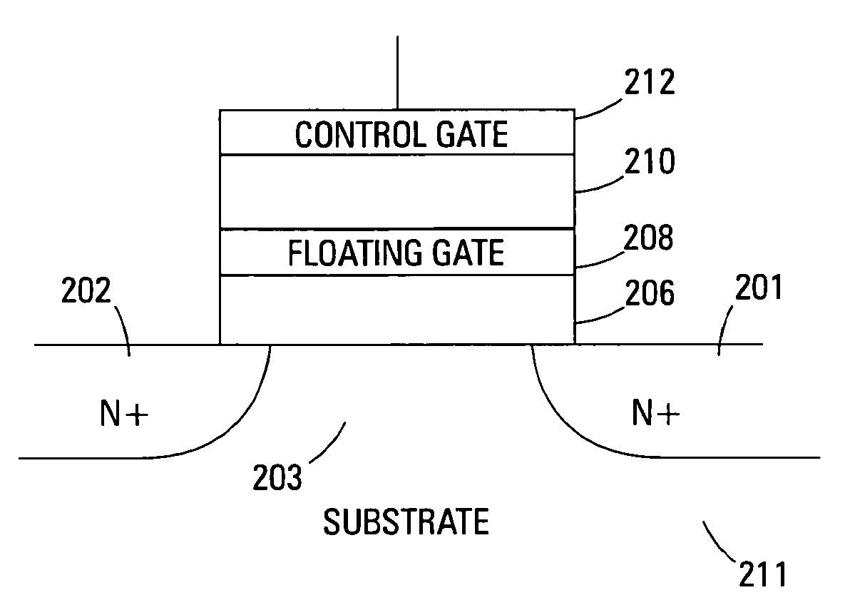
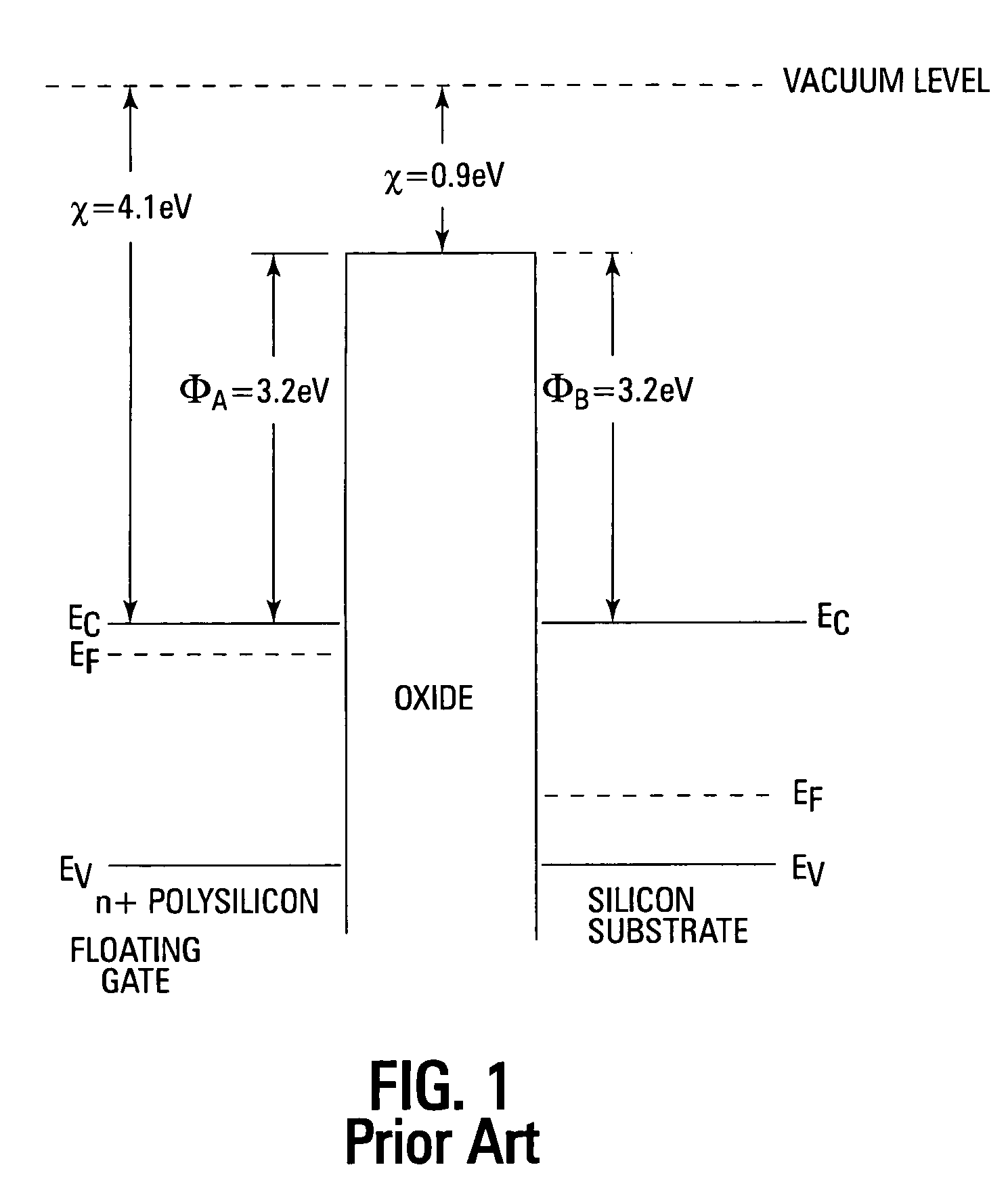
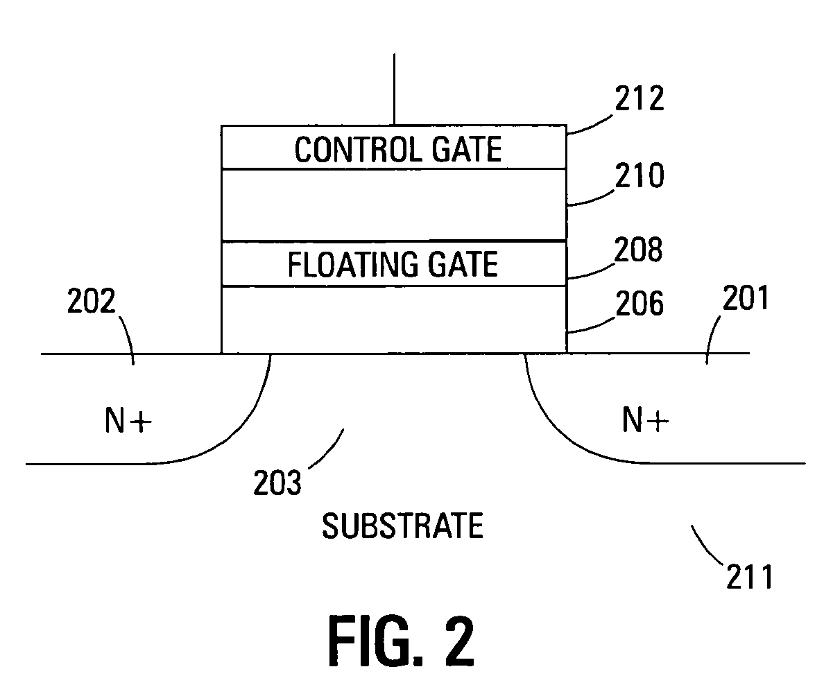
[0021] In the following detailed description of the invention, reference is made to the accompanying drawings that form a part hereof and in which is shown, by way of illustration, specific embodiments in which the invention may be practiced. In the drawings, like numerals describe substantially similar components throughout the several views. These embodiments are described in sufficient detail to enable those skilled in the art to practice the invention. Other embodiments may be utilized and structural, logical, and electrical changes may be made without departing from the scope of the present invention. The following detailed description is, therefore, not to be taken in a limiting sense, and the scope of the present invention is defined only by the appended claims and equivalents thereof. The terms wafer or substrate used in the following description include any base semiconductor structure. Both are to be understood as including silicon-on-sapphire (SOS) technology, silicon-on-...


PUM

PropertyMeasurementUnit
dielectric constantaaaaaaaaaa
band gapaaaaaaaaaa
band gap energyaaaaaaaaaa

Abstract

A graded composition, high dielectric constant gate insulator is formed between a substrate and floating gate in a flash memory cell transistor. The gate insulator is comprised of amorphous germanium or a graded composition of germanium carbide and silicon carbide. If the composition of the gate insulator is closer to silicon carbide near the substrate, the electron barrier for hot electron injection will be lower. If the gate insulator is closer to the silicon carbide near the floating gate, the tunnel barrier can be lower at the floating gate.

Description

TECHNICAL FIELD OF THE INVENTION [0001] The present invention relates generally to memory devices and in particular the present invention relates to flash memory devices with graded composition gate insulators. BACKGROUND OF THE INVENTION [0002] Memory devices are typically provided as internal, semiconductor, integrated circuits in computers or other electronic devices. There are many different types of memory including random-access memory (RAM), read only memory (ROM), dynamic random access memory (DRAM), synchronous dynamic random access memory (SDRAM), and flash memory. [0003] Flash memory devices have developed into a popular source of non-volatile memory for a wide range of electronic applications. Flash memory devices typically use a one-transistor memory cell that allows for high memory densities, high reliability, and low power consumption. Common uses for flash memory include personal computers, personal digital assistants (PDAs), digital cameras, and cellular telephones....

Claims


Application Information

Patent Timeline
Patent Type & Authority Applications(United States)
IPC IPC(8): H01L29/788
CPCH01L29/513H01L29/7881H01L27/11563H01L27/11517H01L21/8239H10B41/00H10B43/00H10B99/00
Inventor FORBES, LEONARDAHN, KIE Y.
Owner MICRON TECH INC
Why Eureka
Try Eureka