Light emitting element and light emitting device and method of manufacturing light emitting element

a technology of light emitting devices and light emitting elements, which is applied in the direction of thermoelectric devices, other domestic articles, solid-state devices, etc., can solve the problems of complex process flow, still many problems, and inability to meet the requirements of forming tft, so as to achieve the effect of increasing the thickness of the layer on the substrate side where tft or the like is formed, high luminous efficiency, and increasing the thickness of the layer other than the light emitting region

Inactive Publication Date: 2006-11-02
SEMICON ENERGY LAB CO LTD
View PDF23 Cites 47 Cited by
  • Summary
  • Abstract
  • Description
  • Claims
  • Application Information

AI Technical Summary

Benefits of technology

[0036] A light emitting element of the present invention includes a light emitting region having a multiple quantum well structure; thus, the luminous efficiency is high.
[0037] Further, the thickness of a layer other than a light emitting region is increased. In particular, the thickness of the layer on a substrate side where a TFT or the like is formed is increased; thus, a light emitting region having a multiple quantum well structure can be formed over a layer in which irregularities due to minute foreign bodies on the electrode surface are reduced. Accordingly, the effects of a multiple quantum well structure can be acquired more efficiently; thus, a light emitting element with high luminous efficiency can be obtained.
[0038] Further, the thickness of a layer other than a light emitting region is increased, so that a light emitting element in which defects such as short circuit between electrodes or the like are reduced can be obtained.
[0039] Further, the thickness of a layer other than a light emitting region can be increased with suppressing increase in the drive voltage.
[0040] Since a light emitting device of the invention has a light emitting element with high luminous efficiency, fewer defects, and low drive voltage, a light emitting device of low power consumption and less defects can be obtained.
[0041] Further, since a multiple quantum well structure can be formed more easily by a method of manufacturing a light emitting element of the present invention as compared with the conventional methods; thus, the throughput can be improved by employing the method of manufacturing a light emitting element according to the invention.

Problems solved by technology

However, there are still many issues.
One of the issues is a reduction in power consumption.
However, the process flow for forming a TFT is very complicated, and minute foreign bodies are easily generated; thus, it is difficult to remove the generated foreign bodies.
In the case where the minute foreign bodies remain on the electrode, the film thickness of the element becomes nonuniform and a good light-emission cannot be obtained.
Accordingly, in the case where a layer of a multiple quantum well structure has minute foreign bodies, there may be a defect in the multiple quantum well structure.
In other words, the multiple quantum well structure itself becomes difficult to be formed, and the effect of the multiple quantum well structure may not be obtained.
However, when the multiple quantum well structure is formed by controlling open / close of the shutter, the film formation takes more time and the throughput may be decreased.

Method used


Image

  • Light emitting element and light emitting device and method of manufacturing light emitting element
  • Light emitting element and light emitting device and method of manufacturing light emitting element
  • Light emitting element and light emitting device and method of manufacturing light emitting element

Examples


embodiment 1

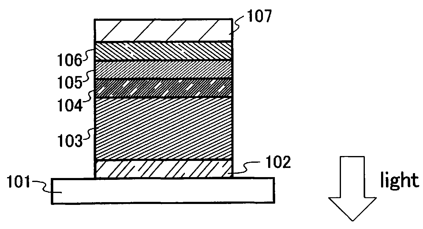
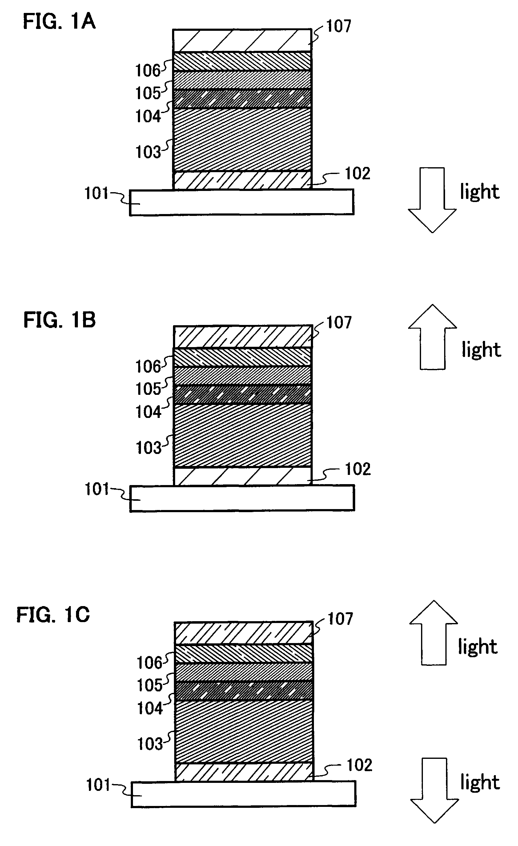
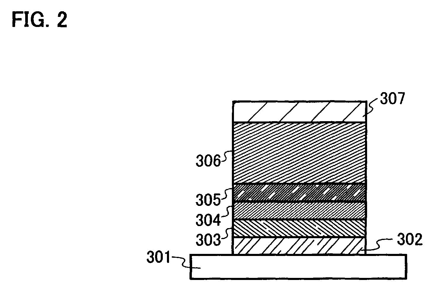
[0059] In this embodiment, a layer containing a composite material used for a light emitting element of the present invention will be described. The layer containing a composite material used for a light emitting element of the invention contains an organic compound and an inorganic compound.

[0060] An organic compound contained in the layer containing a composite material is preferably a material superior in hole transporting property. In particular, an organic compound material having an arylamine skeleton, for example, a compound of aromatic amines (namely, having a benzene ring-nitrogen bond) such as 4,4′-bis (N-{4-[N,N′-bis(3-methylphenyl)amino]phenyl}-N-phenylamino)biphenyl (abbreviated as DNTPD), 4,4′-bis [N-(4-diphenylaminophenyl)-N-phenylamino]biphenyl (abbreviated as DPAB), N,N′-bis(3-methylphenyl)-N,N′-diphenyl-[1,1′-biphenyl]-4,4′-diamine (abbreviated as TPD), 4,4′-bis [N-(1-naphthyl)-N-phenylamino]biphenyl (abbreviated as a-NPD), 4,4′-bis [N-(9,9-dimethylfluorene-2-yl)-...

embodiment 2

[0067] In this embodiment, a light emitting region having a multiple quantum well structure in a light emitting element of the present invention will be described.

[0068] A light emitting region of a light emitting element of the invention has a multiple quantum well structure. Specifically, a material having high carrier transporting property, which is hardly crystallized (hereinafter referred to as a host material), and a material having high light emitting property (hereinafter referred to as a guest material) are combined to form the structure.

[0069] As the material having high carrier transporting property, for example, a silicon compound such as tetraphenylsilane or tetra(3-methylphenyl) silane, an anthracene derivative such as 9,10-diphenylanthracene or 9,10-di(2-naphthyl)anthracene, a bianthryl derivative such as 10,10′-diphenyl 9,9′-dianthracene, a pyrene derivative such as 1,3,6,8-tetraphenylpyrene, a carbazole derivative such as 4,4′-di(N-carbazolyl)biphenyl, an oxazole ...

embodiment 3

[0080] A vapor deposition apparatus used for implementing the present invention and a method of manufacturing a light emitting region having a multiple quantum well structure using the vapor deposition apparatus with reference to FIGS. 12 to 15.

[0081] In the vapor deposition apparatus used in this embodiment, a treatment chamber 1001 in which an object is subjected to vapor deposition and a transferring chamber 1002 are provided. The object is transferred to the treatment chamber 1001 through the transferring chamber 1002. The transferring chamber 1002 is provided with an arm 1003 for carrying the object (FIG. 15).

[0082] As shown in FIG. 12, in the treatment chamber 1001, a holder for fixing an object, an evaporation source 1011a filled with a first material, and an evaporation source 1011b filled with a second material are provided. In FIG. 12, the holder for holding an object includes a first rotating plate 1012, which rotates around an axis 1013, and a plurality of second rotat...


PUM


Abstract

It is an object of the present invention to provide a light emitting element with high luminous efficiency, less defects, and low voltage, and a light emitting device having such a light emitting element. It is another object of the invention to provide a method of manufacturing such a light emitting element in simpler manner compared with a conventional manner. A light emitting element of the present invention includes a pair of electrodes, a layer containing a composite material, and a light emitting region; wherein the layer containing a composite material contains an organic compound and an inorganic compound; the light emitting region contains a material having a high light emitting property and a material having a high carrier transporting property, and a region containing high concentration of the material having a high light emitting property and a region containing high concentration of the material having a high carrier transporting property are alternately stacked in the light emitting region.

Description

BACKGROUND OF THE INVENTION [0001] 1. Field of the Invention [0002] The present invention relates to a light emitting element using electroluminescence and a light emitting device provided with the light emitting element. The invention further relates to a method of manufacturing a light emitting element. [0003] 2. Description of the Related Art [0004] In recent years, a light emitting element using a light emitting organic compound has been actively researched and developed. In a basic structure of this light emitting element, a layer containing a light emitting organic compound is sandwiched between a pair of electrodes. By applying voltage to this element, electrons and holes are separately injected from the pair of electrodes into the layer containing a light emitting organic compound, and current flows. Then, recombination of these carriers (the electrons and holes) causes the light emitting organic compound to form an excited state and to emit light when the excited state retu...

Claims


Application Information

Patent Timeline
Patent Type & Authority Applications(United States)
IPC IPC(8): H01L29/08
CPCH01L51/5012Y10S428/917H10K50/11
Inventor NOMURA, RYOJIARAI, YASUYUKIKATO, KAORUYAMAZAKI, SHUNPEI
Owner SEMICON ENERGY LAB CO LTD
Why Eureka
Try Eureka