A semiconductor light-emitting device, and a method of manufacture of a semiconductor device

Inactive Publication Date: 2006-11-02
SHARP KK
View PDF7 Cites 19 Cited by
  • Summary
  • Abstract
  • Description
  • Claims
  • Application Information

AI Technical Summary

Benefits of technology

[0047] The first layer may be disposed immediately adjacent to the second layer. This places the electron gas region as close as possible to the active region, thereby provi

Problems solved by technology

It is generally undesirable to incorporate a layer of AlN or AlGaN with a high aluminium mole fraction into a device, since this can lead to excessive strain within the device, to the formation of dislocations, and to u

Method used


Image

  • A semiconductor light-emitting device, and a method of manufacture of a semiconductor device
  • A semiconductor light-emitting device, and a method of manufacture of a semiconductor device
  • A semiconductor light-emitting device, and a method of manufacture of a semiconductor device

Examples


Embodiment Construction

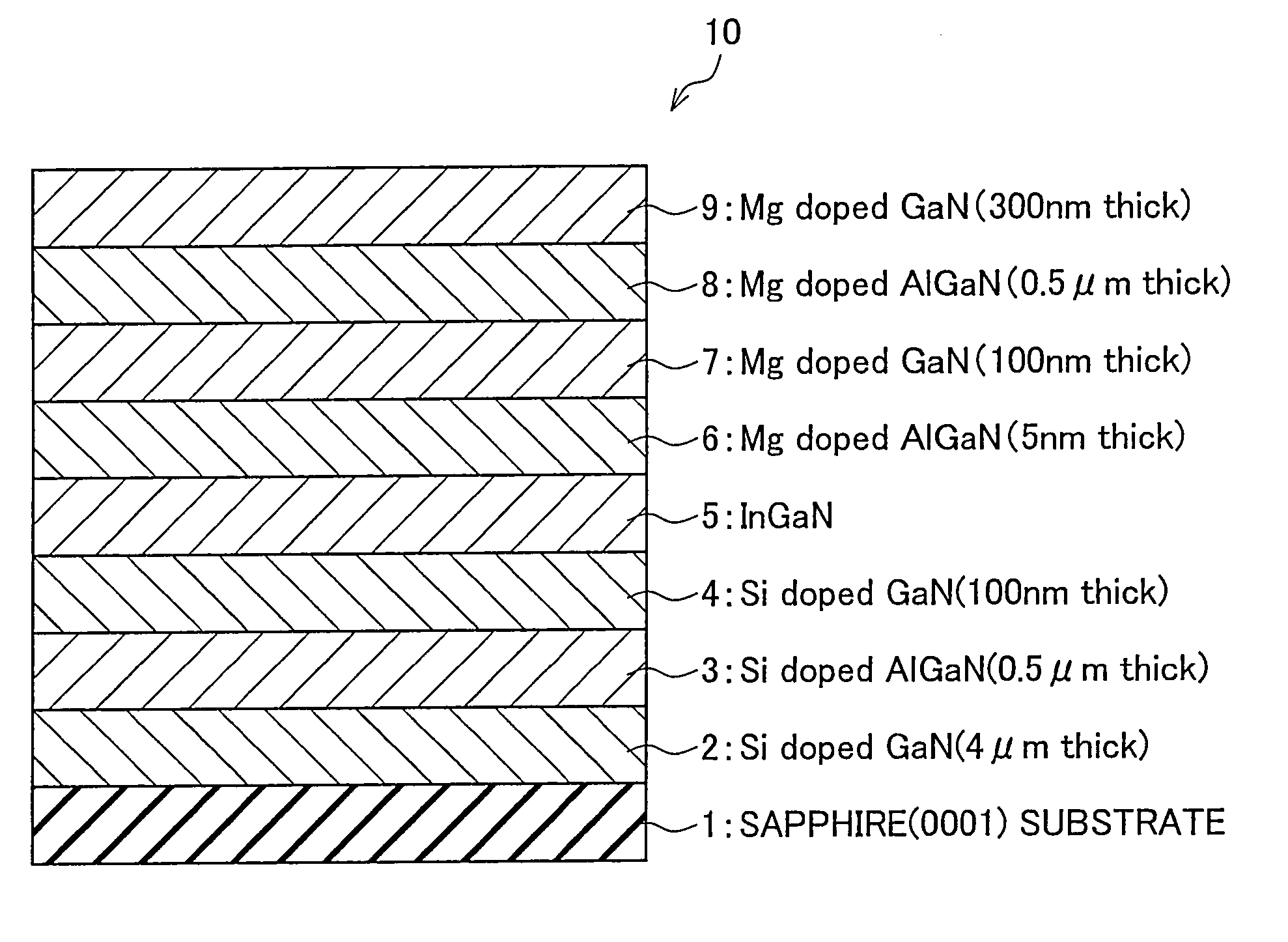
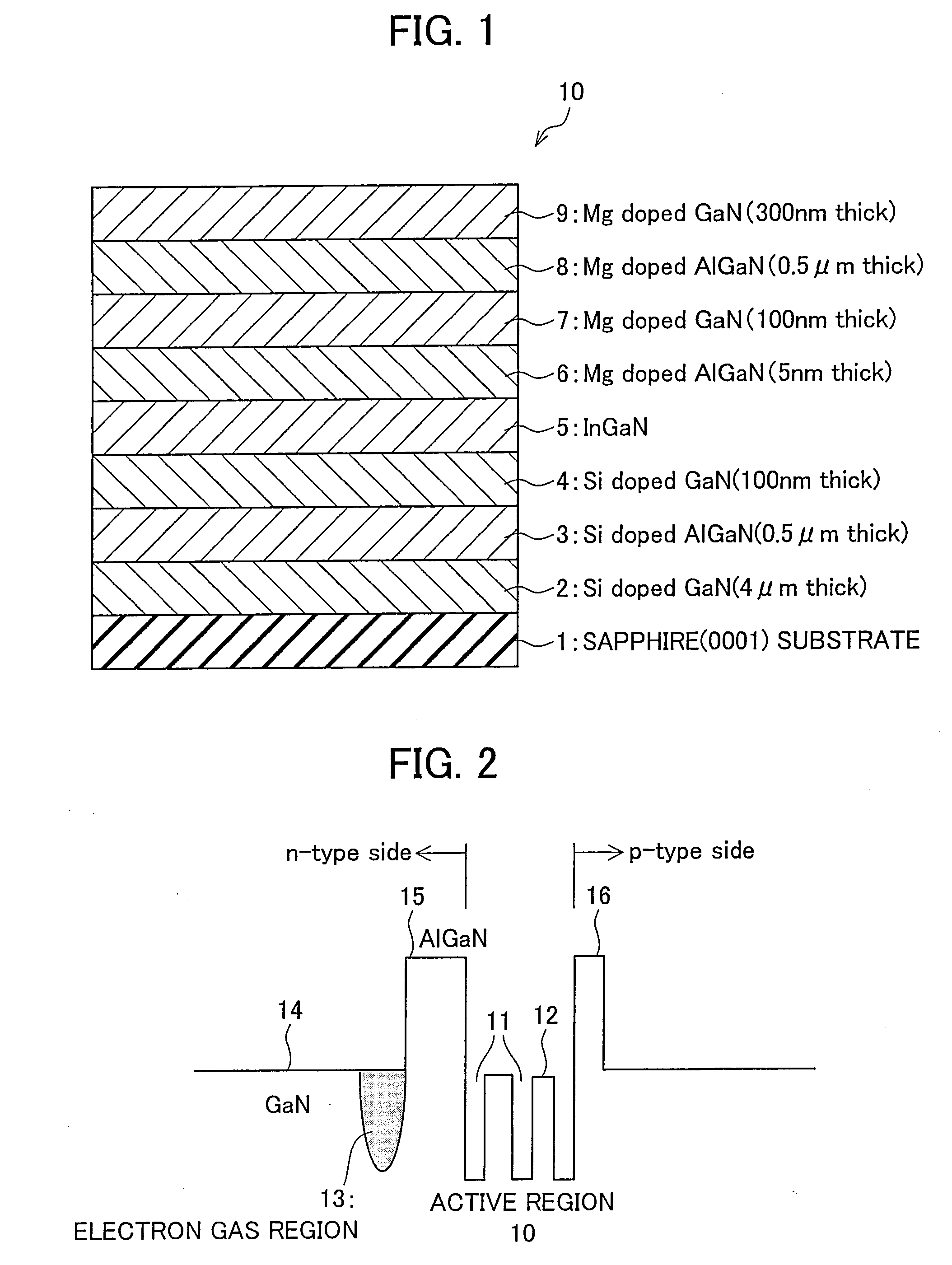
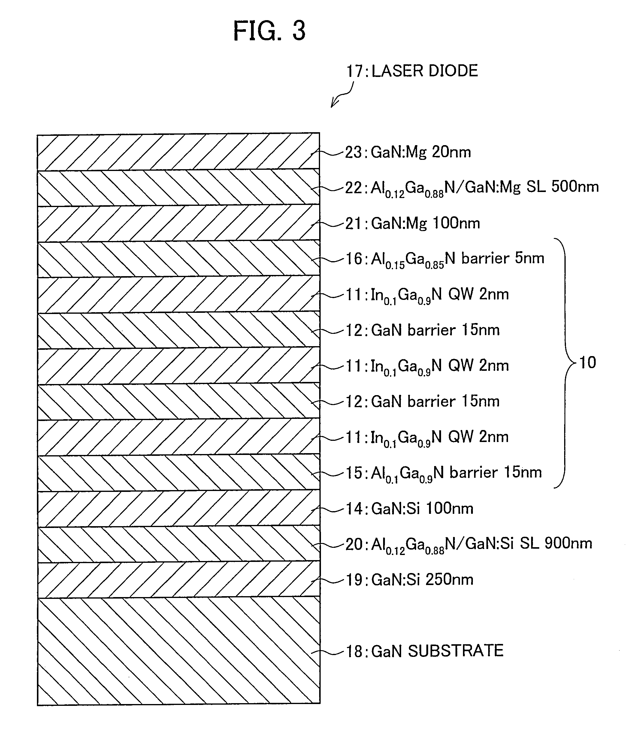
[0062]FIG. 2 is a schematic illustration of the conduction band of a light-emitting device according to one embodiment of the present invention. The device has an active region for light emission. The active region comprises quantum well layers 11, with a barrier layer 12 being disposed between each two adjacent quantum well layers 11. FIG. 2 shows the active region as having three quantum well layers 11 and two barrier layers 12, but the invention is not limited to this specific construction of the active region.

[0063] The active region further comprises a first barrier layer 15 disposed immediately below the lowest quantum well layer 11 and a second barrier layer 16 disposed immediately above the uppermost quantum well layer 11. In the example of FIG. 2, the first and second barrier layers are each an AlGaN layer.

[0064] The portion of the device lying to the left, in FIG. 2, of the active region 10 is the n-type side of the device, and the portion of the device lying to the righ...


PUM


Abstract

A method of manufacturing a nitride semiconductor device comprises the steps of: growing an InxGa1-xN (0≦x≦1) layer, and growing an aluminium-containing nitride semiconductor layer over the InxGa1-xN layer at a growth temperature of at least 500° C. so as to form an electron gas region at an interface between the InxGa1-xN layer and the nitride semiconductor layer. The nitride semiconductor layer is then annealed at a temperature of at least 800° C.
The method of the invention can provide an electron gas having a sheet carrier density of 6×1013 cm−2 or greater. An electron gas with such a high sheet carrier concentration can be obtained with an aluminium-containing nitride semiconductor layer having a relatively low aluminium concentration, such as an aluminium mole fraction of 0.3 or below, and without the need to dope the aluminium-containing nitride semiconductor layer or the InxGa1-xN layer.

Description

[0001] This nonprovisional application claims priority under 35 U.S.C. § 119(a) on Patent Applications No. 0508557.6 and No. 0508556.8, both filed in the U.K. on Apr. 28, 2005, the entire contents of which are hereby incorporated by reference. FIELD OF THE INVENTION [0002] The present invention relates to a semiconductor light-emitting device, and in particular to a semiconductor light-emitting device fabricated in a nitride materials system such as, for example, the (Al,Ga,In)N materials system. The present invention also relates to a method of manufacture of a semiconductor device, and in particular to manufacture of a semiconductor device in a nitride materials system such as, for example, the (Al,Ga,In)N materials system. The invention may be applied to, for example, a light-emitting diode (LED) or to a laser diode (LD), or to manufacture of an optical semiconductor device such as a light-emitting diode (LED) or a laser diode (LD). The invention may also be applied to manufactur...

Claims


Application Information

Patent Timeline
IPC IPC(8): H01L33/00H01L33/02H01L33/32
CPCB82Y20/00H01L21/0242H01L21/02458H01L21/0254H01L29/155H01L29/2003H01S5/34333H01L33/025H01L33/32H01S5/2004H01S5/3063H01S5/3216H01L33/0095
Inventor HOOPER, STEWART EDWARDBOUSQUET, VALERIEHEFFERNAN, JONATHAN
Owner SHARP KK
Why Eureka
Try Eureka