Nitride semiconductor light emitting device and method of manufacturing the same

a light-emitting device and semiconductor technology, applied in the field of nitride semiconductor light-emitting devices, can solve the problems of reducing the yield and reliability affecting the efficiency of the light-emitting device, and the difficulty of forming ohmic contact with the electrode, so as to enhance the current-spreading effect, reduce the operating voltage, and minimize the effect of leakage curren

Inactive Publication Date: 2006-11-09
SAMSUNG ELECTRO MECHANICS CO LTD
View PDF11 Cites 44 Cited by
  • Summary
  • Abstract
  • Description
  • Claims
  • Application Information

AI Technical Summary

Benefits of technology

[0020] An advantage of the present invention is that it provides a nitride semiconductor light emitting device which can reduce an operational voltage and can enhance a current-spreading effect, while minimizing a leakage current due to a reflecting material such as silver.
[0021] Another advantage of the invention is that it provides a method of manufacturing the nitride semiconductor light emitting device.
[0022] Additional aspects and advantages of the present general inventive concept will be set forth in part in the description which follows and, in part, will be obvious from the description, or may be learned by practice of the general inventive concept.
[0023] According to an aspect of the invention, a nitride semiconductor light emitting device includes an n-type electrode; an n-type nitride semiconductor layer that is formed to come in contact with the n-type electrode; an active layer that is formed on the n-type nitride semiconductor layer; a p-type nitride semiconductor layer that is formed on the active layer; an undoped GaN layer that is formed on the p-type nitride semiconductor layer; an AlGaN layer that is formed on the undoped GaN layer so as to provide a two-dimensional electron gas layer to the interface with the undoped GaN layer; a reflecting layer that is formed on the AlGaN layer; a barrier that is formed so as to surround the reflecting layer; and a p-type electrode that is formed on the barrier.
[0024] Preferably, the barrier is formed on the AlGaN layer, and is composed of a first barrier which has a larger thickness than the reflecting layer and a second barrier which is formed on the reflecting layer while coming in contact with the side wall of the first barrier. More preferably, the first barrier is formed of any one selected from a group composed of undoped GaN, SiO2, and SiNx, and the second barrier is formed of Cr / Ni or TiW. Such a construction enhances the adherence between the AlGaN layer and the first barrier formed on the AlGaN layer, thereby preventing the reflecting material of the reflecting layer from being diffused due to an adhesion defect.
[0025] Preferably, the undoped GaN layer has a thickness of 50 to 500 Å, and the Al content of the AlGaN layer is in the range of 10 to 50% in consideration of the crystallinity. In this case, the AlGaN layer has a thickness of 50 to 500 Å in order to form the two-dimensional electron gas layer.

Problems solved by technology

However, since such a nitride semiconductor has a relatively large energy band-gap, it is difficult to form the ohmic contact with an electrode.
However, the reflecting material such as silver (Ag) composing the rear surface reflecting layer is easily diffused.
Such diffusion causes leakage current to be generated, thereby reducing the yield and reliability of the light emitting device.
However, a defect in the contact between the metallic material such as Cr / Ni or TiW composing the barrier 160 and the semiconductor composing the p-type nitride semiconductor layer 140 causes the leakage current of the light emitting device to further increase.
As a result, the characteristic and reliability of the nitride semiconductor light emitting device are deteriorated, and the yield is also reduced.

Method used


Image

  • Nitride semiconductor light emitting device and method of manufacturing the same
  • Nitride semiconductor light emitting device and method of manufacturing the same
  • Nitride semiconductor light emitting device and method of manufacturing the same

Examples


first embodiment

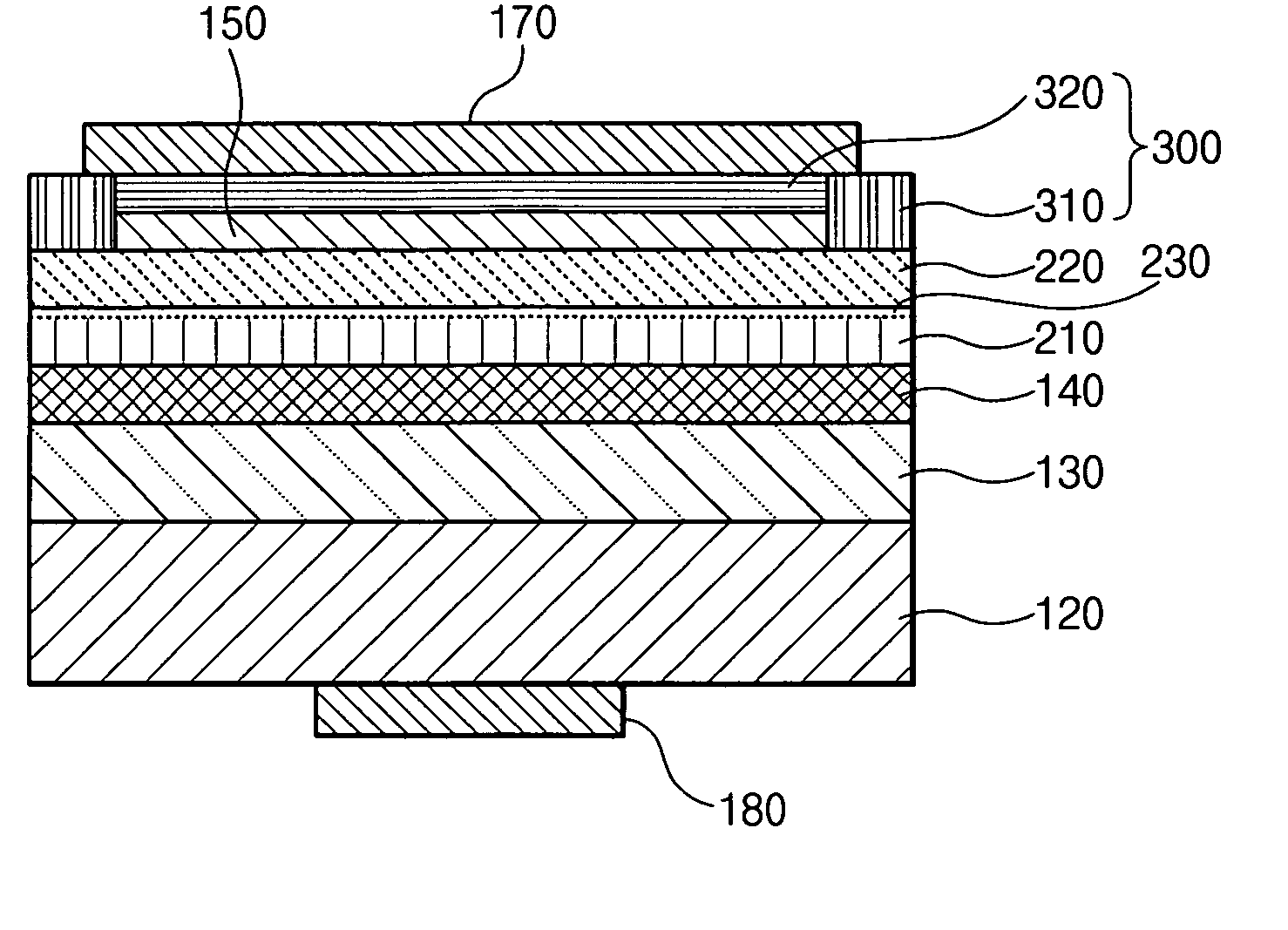
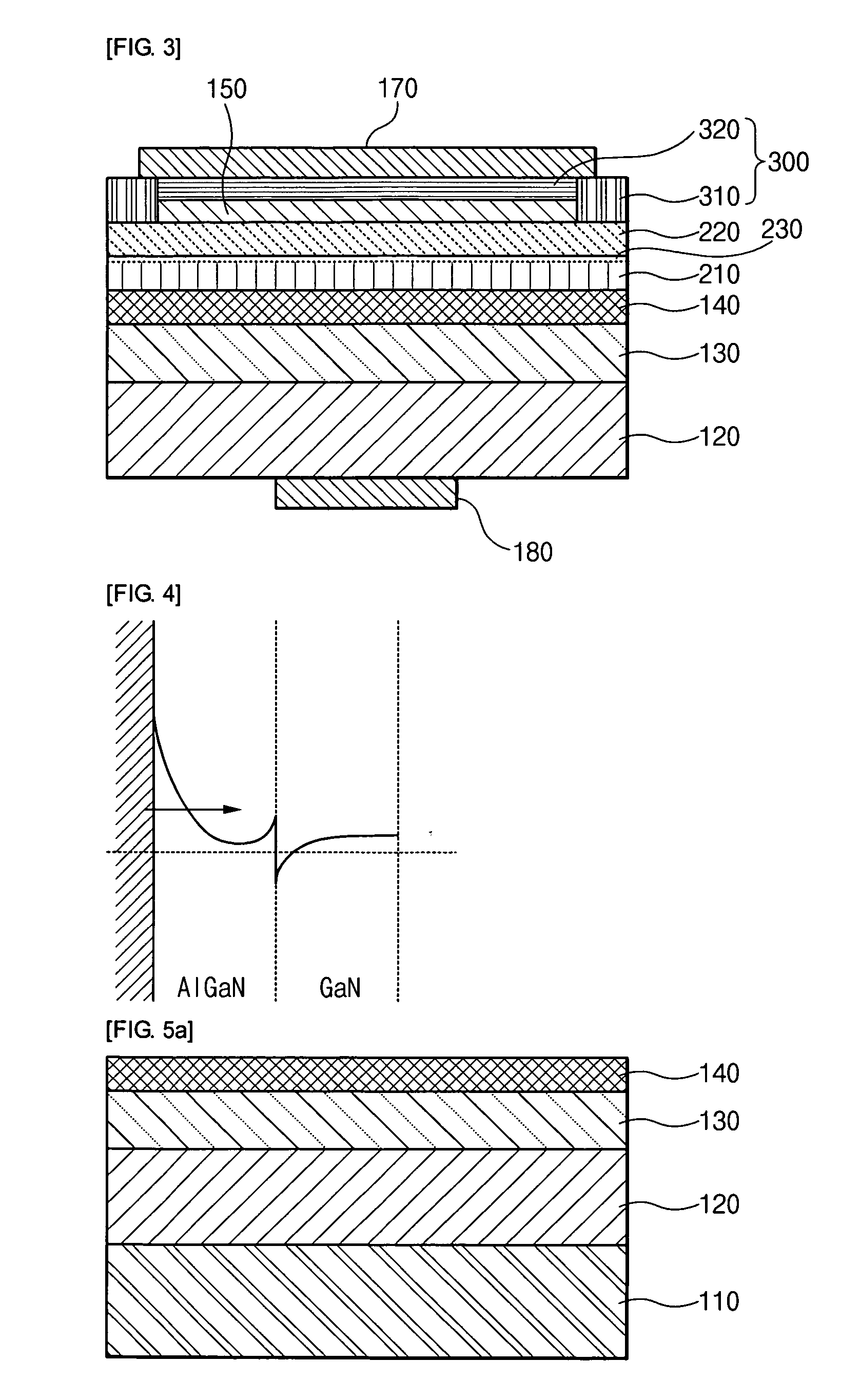
[0047] First, a nitride semiconductor light emitting device according to the invention will be described in detail with reference to FIGS. 3 and 4.

[0048]FIG. 3 is a cross-sectional view illustrating the structure of the nitride semiconductor light emitting device according to the first embodiment of the invention, and FIG. 4 is an energy band diagram showing a heterojunction band structure which is adopted in the nitride semiconductor light emitting device shown in FIG. 3.

[0049] As shown in FIG. 3, an n-type nitride semiconductor layer 120, an active layer 130, and a p-type nitride semiconductor layer 140 are sequentially laminated on an n-type electrode 180.

[0050] The n-type or p-type nitride semiconductor layers 120 or 140 can be formed of a GaN layer or GaN / AlGaN layer which is doped with a conductive impurity. The active layer 130 can have a multi-quantum well structure which is composed of an InGaN / GaN layer.

[0051] On the p-type nitride semiconductor layer 140, a two-dimensi...

second embodiment

[0088]FIG. 6 is a cross-sectional view illustrating the structure of a nitride semiconductor light emitting device according to the

[0089] As described in FIG. 6, the construction of the nitride semiconductor light emitting device according to the second embodiment is almost the same as that of the nitride semiconductor light emitting device according to the first embodiment. However, the n-type electrode 180 is not formed on the rear surface of the n-type nitride semiconductor layer 120 on which the active layer is formed, but is formed on a surface which is exposed by removing portions of the active layer 130, the p-type nitride semiconductor layer 140, the undoped GaN layer 210, and the AlGaN layer 220, that is, on the n-type nitride semiconductor layer 120 on which the active layer is formed. On the rear surface of the n-type nitride semiconductor layer 120, the sapphire substrate 110 is formed to come in contact with the n-type nitride semiconductor layer.

[0090] In other words,...


PUM


Abstract

The present invention relates to a nitride semiconductor light emitting device. The nitride semiconductor light emitting device includes an n-type electrode; an n-type nitride semiconductor layer that is formed to come in contact with the n-type electrode; an active layer that is formed on the n-type nitride semiconductor layer; a p-type nitride semiconductor layer that is formed on the active layer; an undoped GaN layer that is formed on the p-type nitride semiconductor layer; an AlGaN layer that is formed on the undoped GaN layer so as to provide a two-dimensional electron gas layer to the interface with the undoped GaN layer; a reflecting layer that is formed on the AlGaN layer; a barrier that is formed so as to surround the reflecting layer; and a p-type electrode that is formed on the barrier.

Description

CROSS-REFERENCE TO RELATED APPLICATIONS [0001] The application claims the benefit of Korea Patent Application No. 2005-0037056 filed with the Korea Industrial Property Office on May 3, 2005, the disclosure of which is incorporated herein by reference. BACKGROUND OF THE INVENTION [0002] 1. Field of the Invention [0003] The present invention relates to a nitride semiconductor light emitting device and a method of manufacturing the same, and more specifically, to a nitride semiconductor light emitting device which can reduce an operational voltage and enhance a current-spreading effect, while minimizing a current leakage due to a reflecting material such as silver, and a method of manufacturing the same. [0004] 2. Description of the Related Art [0005] In general, a nitride semiconductor is such a material that has a relatively high energy band gap (in the case of GaN semiconductor, about 3.4 eV), and is positively adopted in a light emitting device for generating green or blue short-wa...

Claims


Application Information

Patent Timeline
Patent Type & Authority Applications(United States)
IPC IPC(8): H01L33/00H01L33/14H01L33/10H01L33/32H01L33/42H01L33/44
CPCH01L33/14H01L33/405H01L33/32B23P19/006B23P19/002B23P19/06
Inventor LEE, JAE HOONBACK, HYUNG KYKONG, MOON HEON
Owner SAMSUNG ELECTRO MECHANICS CO LTD
Why Eureka
Try Eureka