Heat dissipating structure and light emitting device having the same

a heat dissipating structure and light-emitting technology, applied in semiconductor lasers, semiconductor/solid-state device details, lasers, etc., can solve the problems of reducing the output power of high-output laser diodes with high injection current, difficult to effectively dissipate heat, and affecting so as to prevent the degradation of light-emitting elements and improve the efficiency of heat dissipation. , the effect o

Inactive Publication Date: 2006-11-09
SAMSUNG ELECTRONICS CO LTD
View PDF14 Cites 23 Cited by
  • Summary
  • Abstract
  • Description
  • Claims
  • Application Information

AI Technical Summary

Benefits of technology

[0009] The present disclosure provides a heat dissipating structure designed to prevent degradation of a light-emitting element while providing stable light emission characteristics and a light-emitting device having the heat dissipating structure.
[0010] According to an aspect of the present disclosure, there is provided a heat dissipating structure that is flip-chip bonded to a light-emitting element and facilitates heat dissipation, the heat dissipating structure including: a submount facing the light-emitting element and having at least one groove; a conductive material layer filled into at least a portion of the at least one groove; and a solder layer interposed between the light-emitting element and the submount for bonding. The conductive material layer may contain at least one of gold (Au), copper (Cu), copper (Cu) alloy, copper-tungsten (Cu—W) alloy, silver (Ag), and aluminum (Al) alloy.

Problems solved by technology

However, because most of the heat transferred to the submount 11 tends to concentrate on region A of narrow width being in contact with the solder layer 19, it is difficult to effectively dissipate heat.
Since threshold current for light emission from a laser diode and laser mode stability decrease as temperature increases, a conventional light-emitting device suffers degradation in light emission characteristics of laser over time.
Along with this problem, a high output power laser diode with high injection current also suffers restriction on increase of output power because it generates a large amount of heat.

Method used


Image

  • Heat dissipating structure and light emitting device having the same
  • Heat dissipating structure and light emitting device having the same
  • Heat dissipating structure and light emitting device having the same

Examples


first embodiment

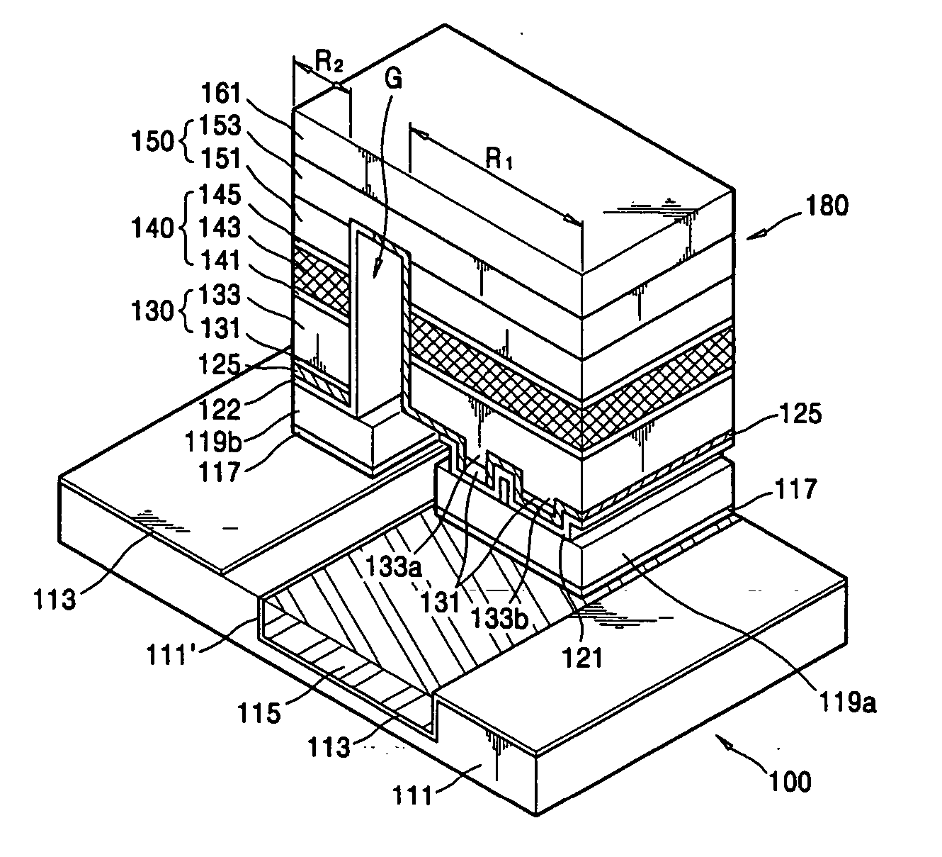
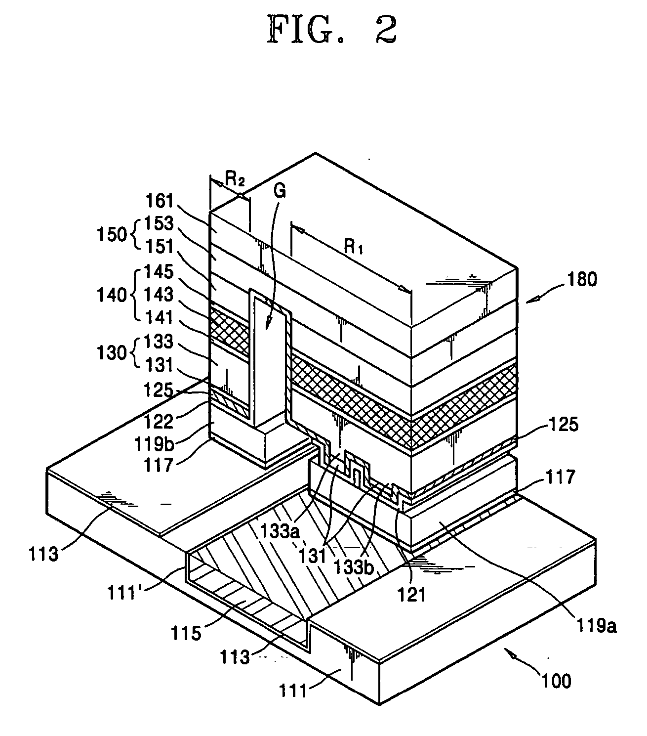
[0026] The present invention will now be described more fully with reference to the accompanying drawings, in which exemplary embodiments of the invention are shown. Referring to FIG. 2, a light-emitting device according to the present disclosure includes a light-emitting element 180 and a heat dissipating structure 100 that are flip-chip bonded to vertically face each other. The light-emitting element 180 includes a substrate 161 forming a base, and an upper material layer 150, a resonant layer 140 and a lower material layer 130 sequentially formed beneath the substrate 161. Here, the structure of the layers formed beneath the substrate 161 is divided into a first area R1 and a second area R2 separated from the first area R1 by a gap G.

[0027] The substrate 161 may be formed of sapphire or III-V compound semiconductor such as gallium nitride (GaN) or silicon carbide (SiC). The upper material layer 150 is formed beneath the substrate 161 and includes a first compound semiconductor la...

second embodiment

[0042]FIG. 4 is a perspective view of a light-emitting device according to the present disclosure. Referring to FIG. 4, like the light-emitting device of FIG. 2, the light-emitting device includes a light-emitting element 280 and a heat dissipating structure 200 flip-chip bonded to the light-emitting element 280. The light-emitting element 280 includes a substrate 261, and an upper material layer 250, a resonant layer 240 and a lower material layer 230 sequentially formed beneath the substrate 261 at first area R1. The upper material layer 250 has a stepped structure that extends to a second area R2. The resonant layer 240 allows laser light to oscillate due to light energy created by recombination of carriers and the upper and lower material layers 250 and 230 are electrically connected to n- and p-type electrodes 222 and 221, respectively. The p-type electrode 221 is formed in the lowermost portion of the first area R1 and coupled to the lower material layer 230 exposed by a curre...

third embodiment

[0047]FIG. 5 is a perspective view of a light-emitting device according to the present disclosure. Like reference numerals in FIGS. 2 and 5 denote like elements. Referring to FIG. 5, a submount 311 has a first groove 311′a formed along one direction and a plurality of second grooves 311′b arranged perpendicular to the length of the first groove 311′a. The first and second grooves 311′a and 311′b are filled with a conductive material layer 315 that rapidly diffuses heat along the plane of the submount 311. The conductive material layers 315 are formed in the two orthogonal directions to facilitate two-dimensional heat diffusion. The heat transferred to the submount 311 is dissipated by natural convection through the outer surface of the submount 311. In this case, heat uniformly transferred to the entire outer surface of the submount 311 is efficiently dissipated through a wide heat transfer area. A metal medium layer 313 may be formed between the conductive material layer 315 and th...


PUM


Abstract

A heat dissipating structure is flip-chip bonded to a light-emitting element and facilitates heat dissipation. The heat dissipating structure includes: a submount facing the light-emitting element and having at least one groove; a conductive material layer filled into at least a portion of the at least one groove; and a solder layer interposed between the light-emitting element and the submount for bonding. The heat dissipating structure and the light-emitting device having the same allow efficient dissipation of heat generated in the light-emitting element during operation.

Description

CROSS-REFERENCE TO RELATED PATENT APPLICATION [0001] Priority is claimed to Korean Patent Application No. 10-2005-0037852, filed on May 6, 2005, in the Korean Intellectual Property Office, the disclosure of which is incorporated herein in its entirety by reference. BACKGROUND OF THE DISCLOSURE [0002] 1. Field of the Disclosure [0003] The present disclosure relates to a heat dissipating structure and a light-emitting device including the same, and more particularly, to a light emitting device including a light-emitting element such as a laser diode (LD) or a light-emitting diode (LED) and a heat dissipating structure that is flip-chip bonded to the light-emitting element to facilitate heat dissipation. [0004] 2. Description of the Related Art [0005] Laser light emitted from a laser diode, one type of light-emitting element, has many practical applications in fields such as optical communications, multiple communications, and space communications. This is due in part to its small freq...

Claims


Application Information

Patent Timeline
Patent Type & Authority Applications(United States)
IPC IPC(8): H01L33/00H01L33/06H01L33/32H01L33/62H01L33/64H01S5/023H01S5/0233
CPCB82Y20/00H01L33/642H01L33/647H01S5/02236H01S5/34333H01S5/02272H01S5/02276H01S5/02492H01S5/22H01S5/0224H01S5/0234H01S5/0237H01S5/02345H01S5/023H01S5/0233H01S5/0235H01S5/024
Inventor CHAE, SU-HEEJANG, TAE-HOONKIM, HYUNG-KUNSUNG, YOUN-JOON
Owner SAMSUNG ELECTRONICS CO LTD
Why Eureka
Try Eureka