

Semiconductor device
a technology of semiconductor devices and semiconductors, applied in semiconductor devices, semiconductor/solid-state device details, electrical apparatus, etc., can solve problems such as shortage in photoresist exposure areas, new issues, and excessive lateral chip size, so as to reduce mutual inductance, reduce mutual inductance, and increase mutual inductance
- Summary
- Abstract
- Description
- Claims
- Application Information
AI Technical Summary
Benefits of technology
Problems solved by technology
Method used
Image

Examples
first embodiment
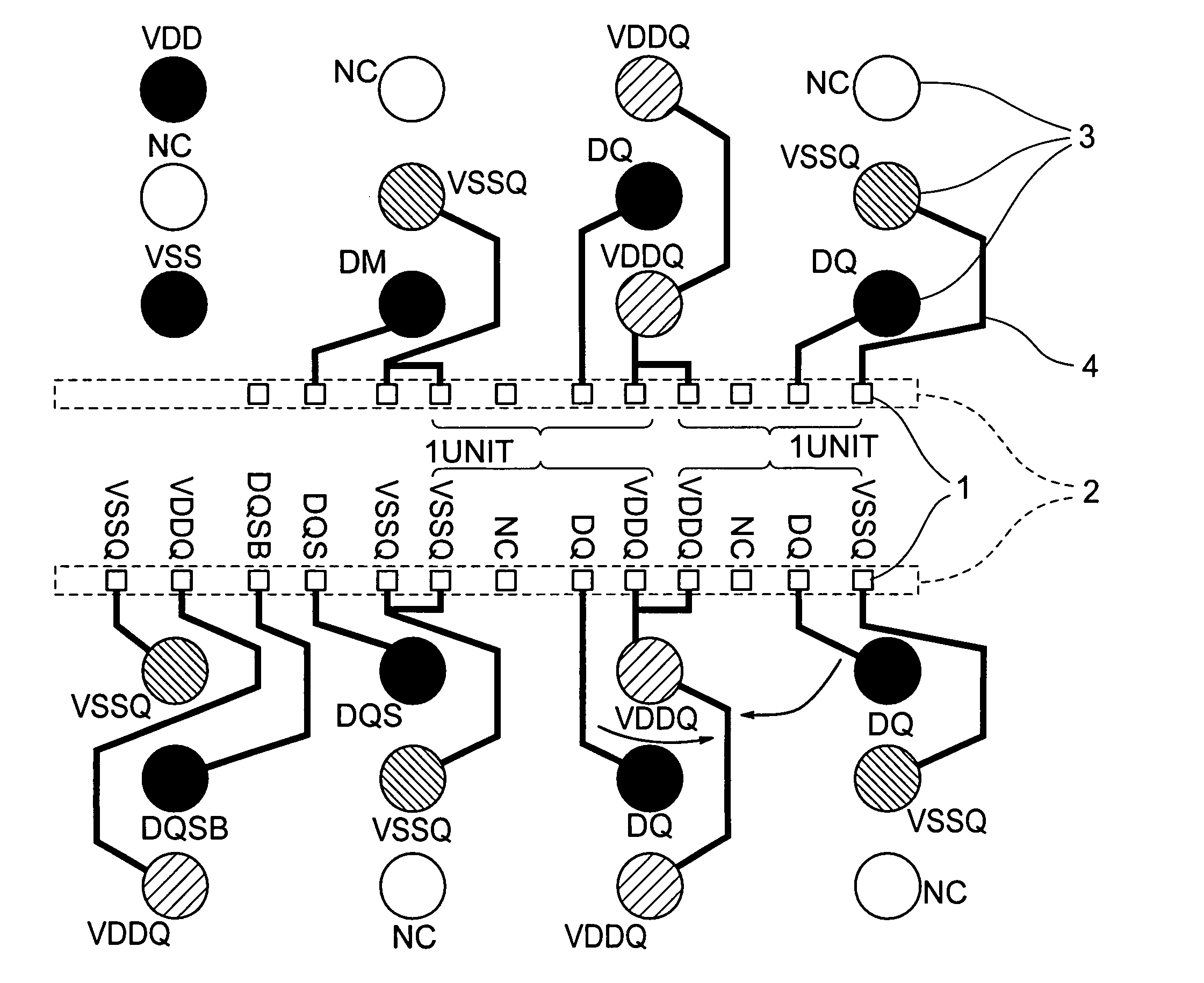
[0048]FIG. 1 is a pad layout of an 8-bit component of a first embodiment according to the present invention. FIG. 1 typically shows pads 1 of a semiconductor chip, solder ball lands 3 of a BGA substrate, and lead wires 4 by which the pads 1 and the solder ball lands 3 are connected to each other. Here, symbols “DQ”, “VDDQ” and “VSSQ” designating data, the data power source and data ground will also be used for solder balls (pins) and lands of the package, and for pads and lead wires of the semiconductor chip unless no particular confusion is caused.
[0049] In FIG. 1, the semiconductor chip has a central area on which pad layouts each including a plurality of pads 1 are disposed in upper and lower areas in two rows. The pads of the upper pad layout 2-1 are wire bonded to the solder ball lands 3 formed in the upper area, respectively, and the pads of the lower pad layout 2-2 are wire bonded to the solder ball lands 3 formed in the lower area, respectively.
[0050]FIG. 1 also typically s...
third embodiment
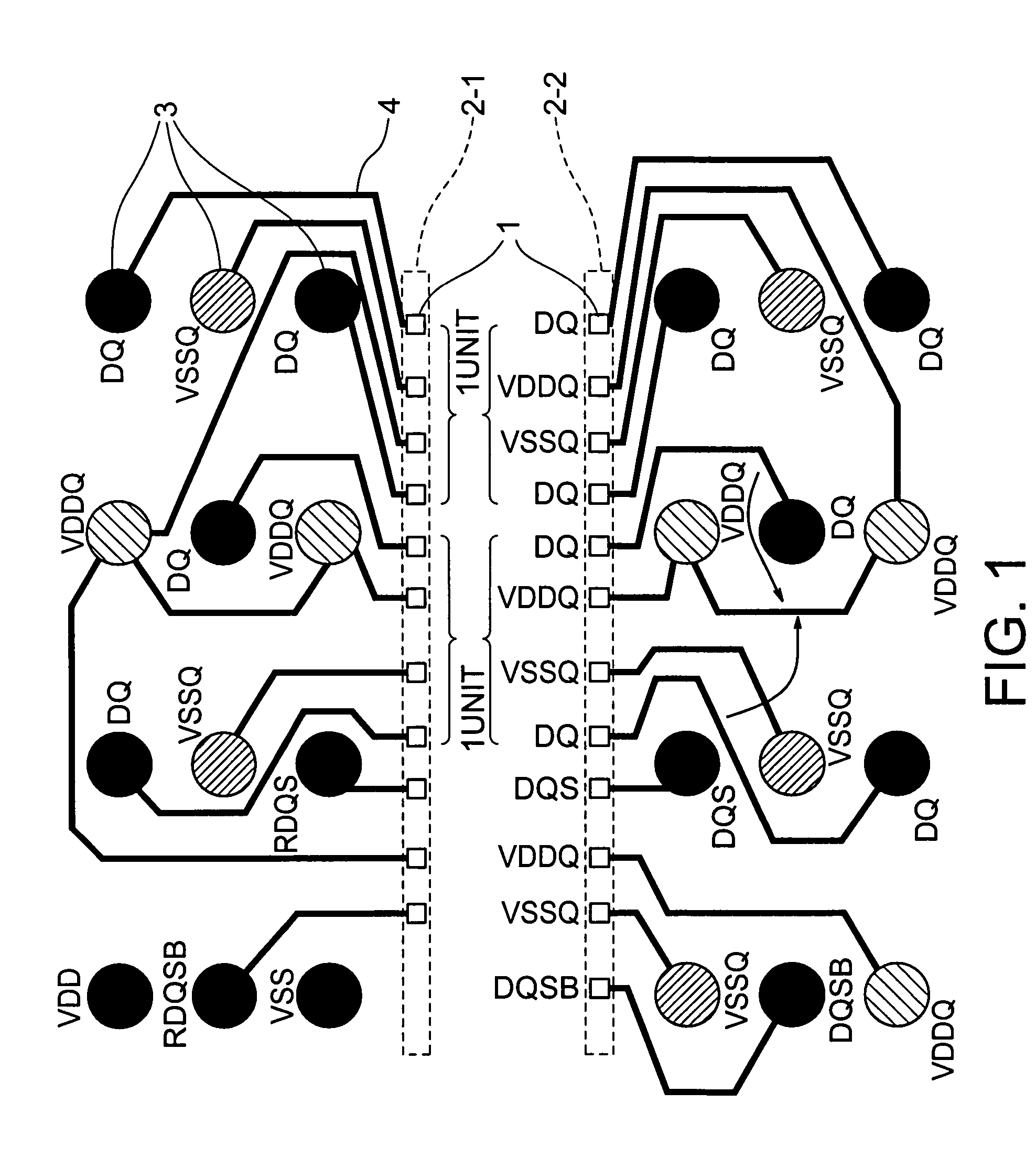
[0060]FIG. 3 shows a layout of a 4-bit component of a third embodiment according to the present invention. In FIG. 3, the 4-bit component can be structured upon removing unnecessary data bits from the structure of FIG. 1. With such a layout, the pads for the solder ball lands 3 corresponding to four pieces of data of a semiconductor chip remain under “NC (Non Connection)” and the land of the data strobe signal RDQS is converted to a data mask DM (Data Mask) signal. Among the 8 pads placed in the pad layout of S-G-V-S and the consecutive pad layout of S-V-G-S of the 8-bit component, the pads S on both ends are held under “NC” to provide six pads in layouts G-V-S and S-V-G. With such a structure, the pads for data power source (VDDQ) and data ground (VSSQ) are wire bonded in the same pattern as that of the 8-bit component.
[0061] In general practice, the 4-bit component employs the same semiconductor chip as that of the 8-bit component and product change is made upon selecting, for ins...
second embodiment
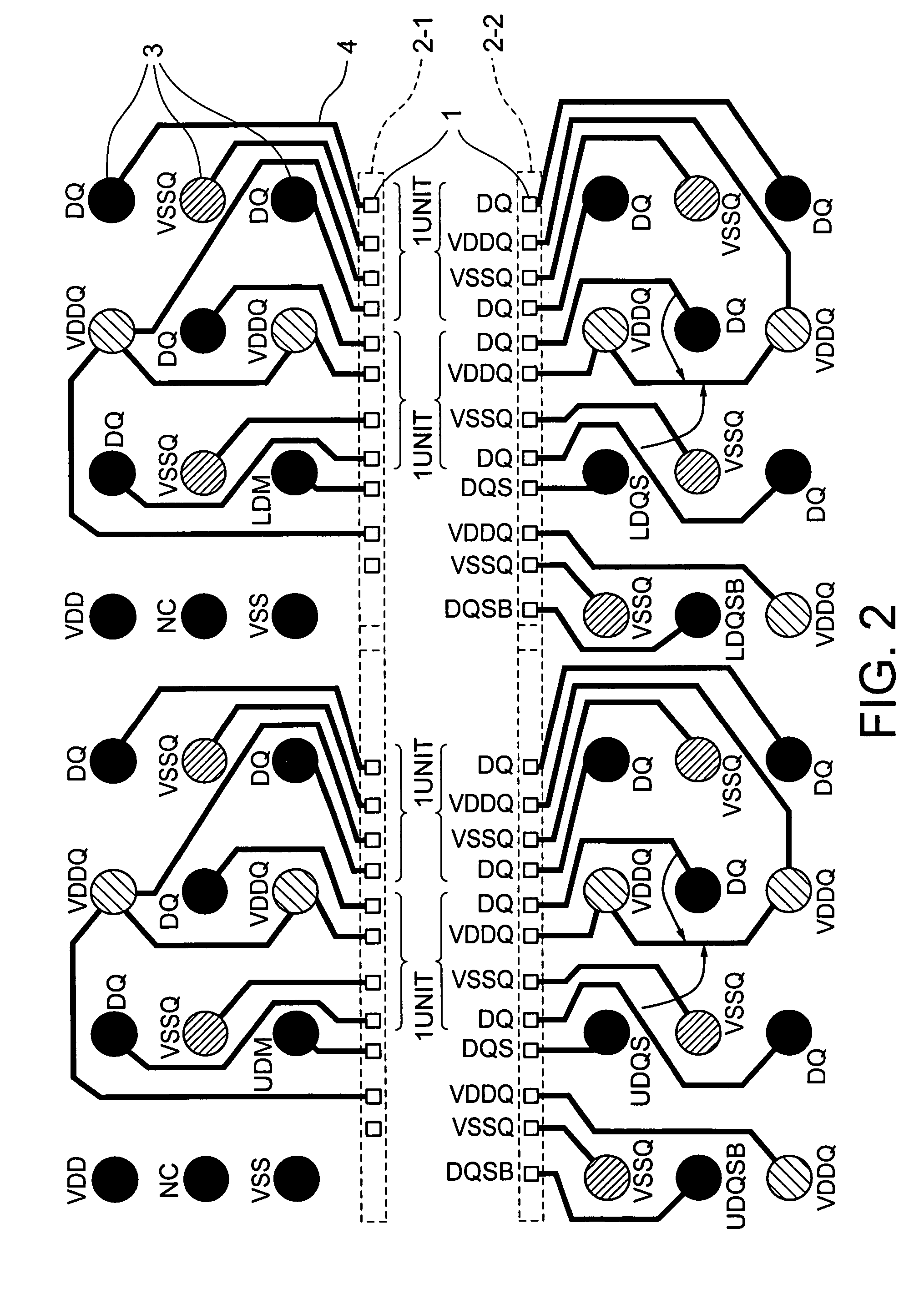
[0064] With the pads shown in FIG. 4, the data ground (VSSQ), data (DQ), the data power source (VDDQ) and data (DQ) are formed in one unit and the 8-bit component includes a unit in layout of G-S-V-S and the other unit in layout of S-V-S-G. The data ground (VSSQ) and the data power source (VDDQ) are located between which data (DQ) is sandwiched. With such a structure, no parallel placement of the data power sources (VDDQ) are achieved with the resultant reduction in mutual inductance between the data power sources (VDDQ) and increase in mutual inductance between the data power source and ground. This results in reduction of effective inductance between the data power source (VDDQ) and ground (VSSQ) and noises of the data power source and ground can be minimized whereby a semiconductor device available to achieve high-speed data transmission can be obtained. Moreover, by repeatedly placing the pad layout of the 8-bit structure shown in FIG. 4 in the same manner as the second embodime...
PUM
 Abstract
Description
Claims
Application Information