Circuit for producing a data bit inversion flag

a technology of inversion flag and circuit, which is applied in the direction of code conversion, instruments, machine control, etc., can solve the problems of data corruption, increased capacitive coupling, and becoming ever more difficult to transmit data from the memory chip to the controller

Active Publication Date: 2006-11-23
POLARIS INNOVATIONS
View PDF6 Cites 10 Cited by
  • Summary
  • Abstract
  • Description
  • Claims
  • Application Information

AI Technical Summary

Problems solved by technology

The increasing operating frequency means that the inductive and capacitive coupling is increased, so that data corruptions arise.
As the operating frequency increases, it becomes ever more difficult to transmit the data from the memory chip to the controller.
A limitation in this context is the noise on the data lines of the data bus.
The noise limits the validity period of the data and reduces the “data eye size”.
The more switching operations or data transitions occur on the data lines, the more the data corruptions increase, i.e. the bit error rate (BER) rises.
The increased waiting time results in an unwanted delay in

Method used


Image

  • Circuit for producing a data bit inversion flag
  • Circuit for producing a data bit inversion flag
  • Circuit for producing a data bit inversion flag

Examples


Embodiment Construction

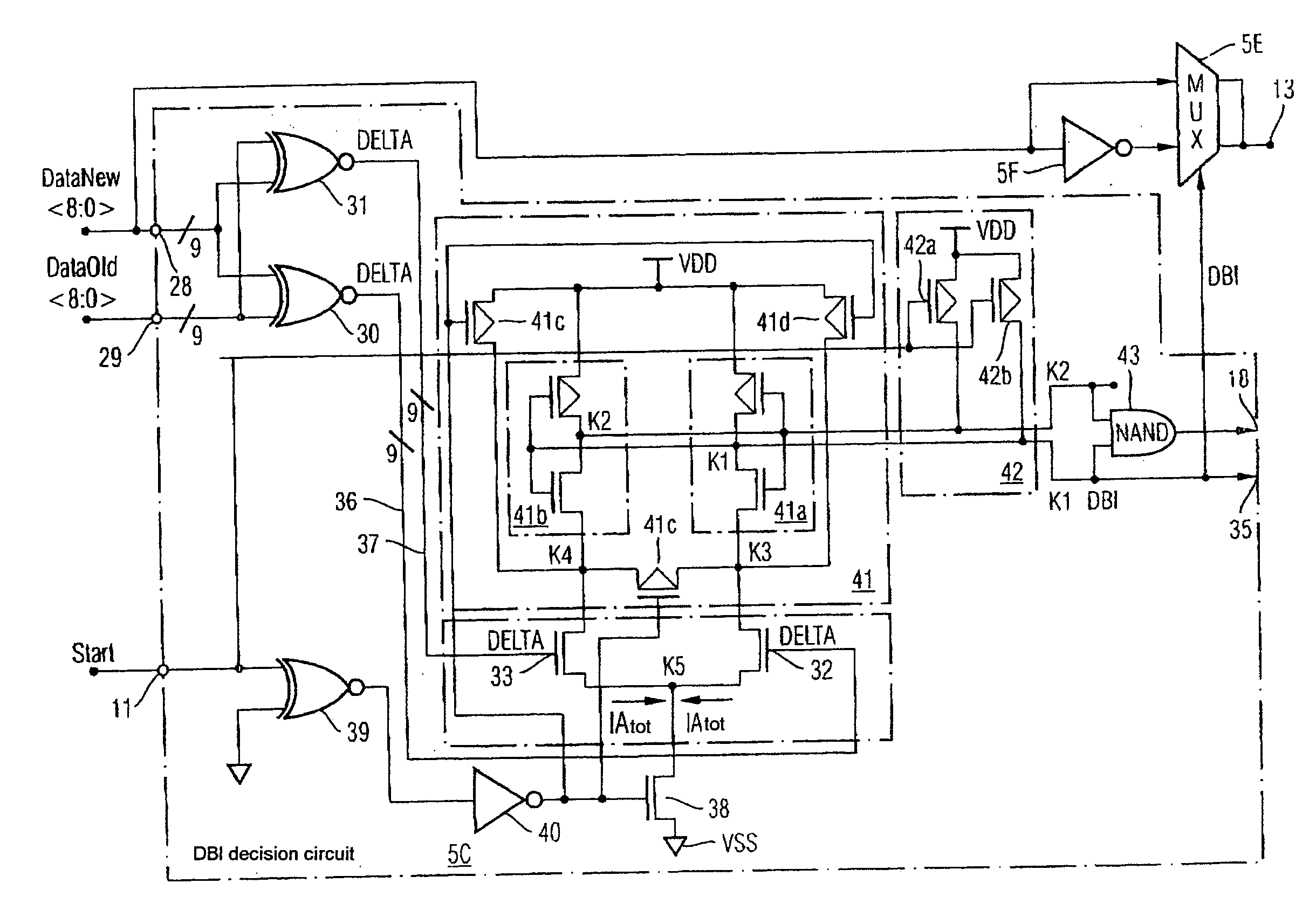
[0068]FIG. 7 shows a first embodiment of a circuit unit 1 for data bit inversion in a data burst which has been read from a memory chip, which embodiment contains a circuit for producing a data bit inversion flag (DBI) based on the invention. The circuit unit 1 is integrated within the memory chip and forms part of the read signal path. The memory chip contains a memory cell array 2 having a multiplicity of memory cells for storing data bits. An internal data bus 3 is used to buffer-store all the data bits from a data burst which is to be read in a burst buffer store 4 in the circuit unit 1. If the data burst comprises m data words each containing n data bits, m n data bits are simultaneously written to the burst buffer store 4. The circuit unit 1 contains a decoding unit 5 which comprises a plurality of decoders 5-i connected up in parallel. For each data word DWi, an associated decoder 5-i is provided within the decoder unit 5. Each decoder 5-i respectively compares the associated...


PUM


Abstract

A circuit for producing a data bit inversion flag comprises a first summed-current production unit for producing a first summed current, whose amplitude is proportional to the number of different data bits in two adjacent data words in a data burst, a second summed-current production unit for producing a second summed current, whose amplitude is proportional to the number of identical data bits in the two adjacent data words, and a current comparator comparing the first with the second summed current and producing a data bit inversion flag if the first summed current is greater than the second summed current.

Description

BACKGROUND OF THE INVENTION [0001] 1. Field of the invention [0002] The invention relates to a circuit for producing a data bit inversion flag for the purpose of data inversion for a data burst which has been read from a memory chip, in particular for DDR-SDRAMs (Double Data Rate Synchronous Dynamic Random Access Memories). [0003] 2. Description of the Prior Art [0004]FIG. 1 shows a computer system based on the prior art in which a memory chip and a controller chip interchange data via a common data bus. The increasing speed of computer processors or controllers requires a correspondingly higher speed for memory access operations or faster memory chips. The memory chip and the processor are clocked by means of a clock signal CLK. [0005] Various generations of RAM stores have been developed, whose access rate rose constantly. The intervals of time in which new data which are read from the memory cell array or which are to be written are available at the data inputs / outputs of the mem...

Claims


Application Information

Patent Timeline
IPC IPC(8): G06F7/02
CPCG11C7/1006G11C7/109G11C7/1078G06F7/00G06F12/00
Inventor HEIN, THOMAS
Owner POLARIS INNOVATIONS
Why Eureka
Try Eureka