

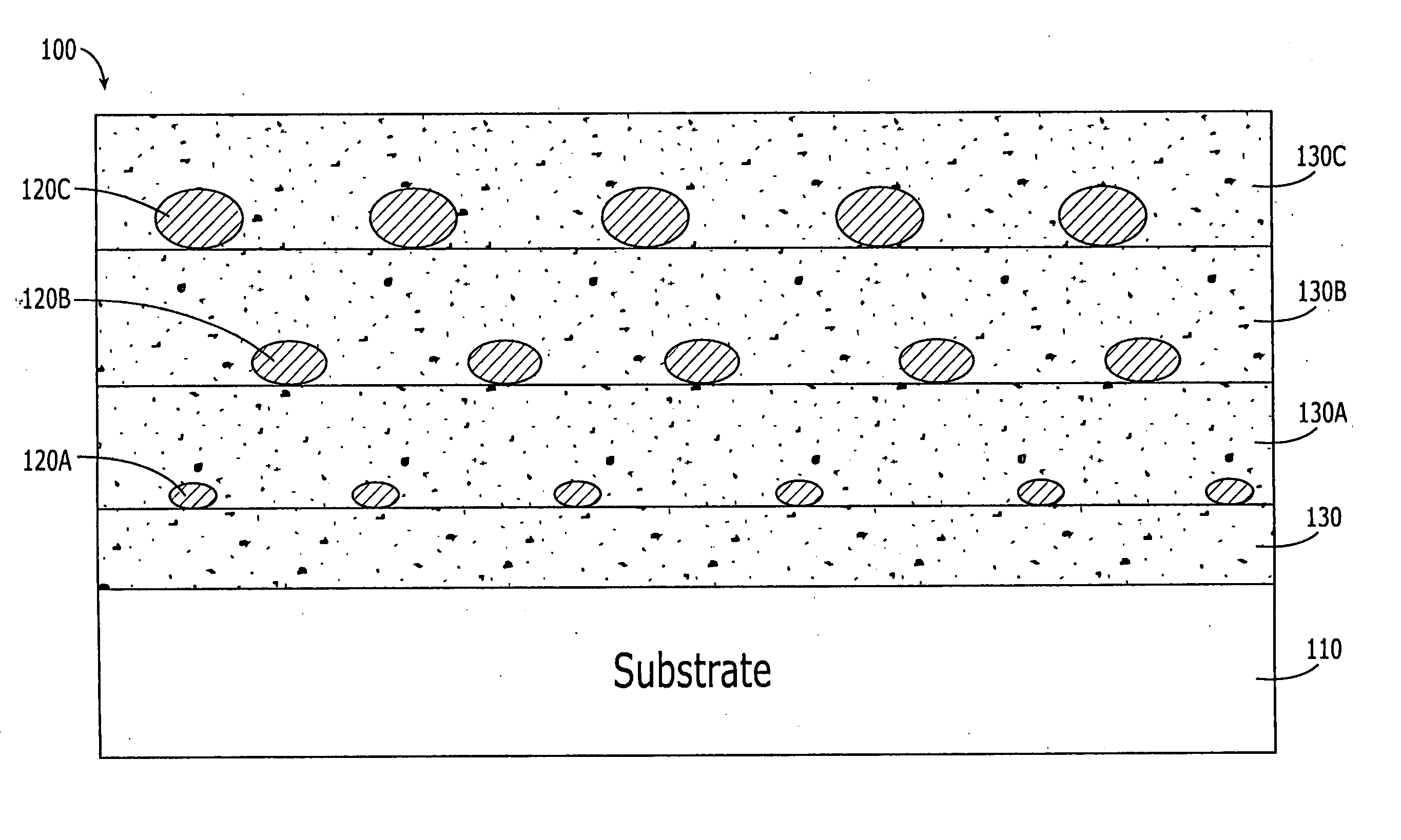
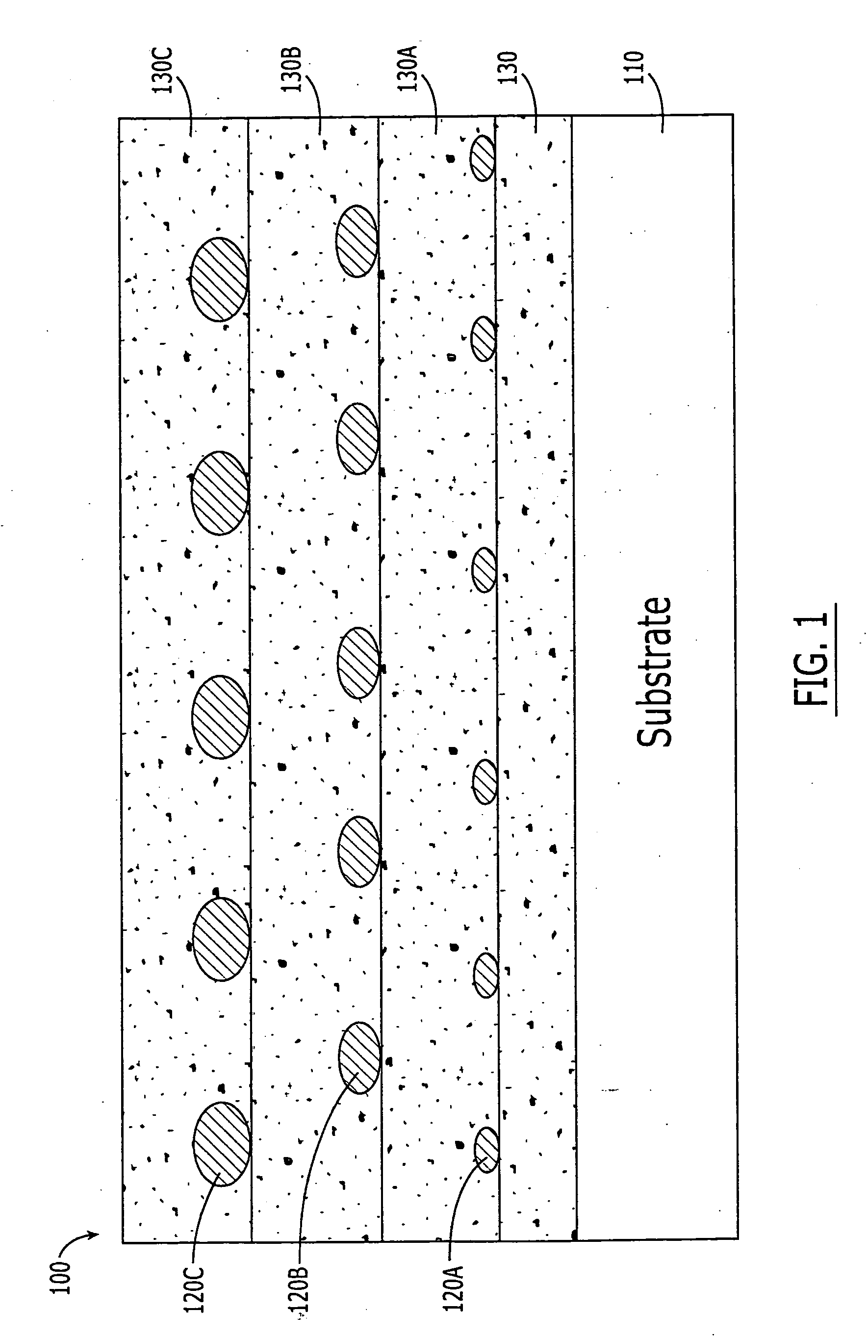
Methods of forming three-dimensional nanodot arrays in a matrix
a nanodot array and matrix technology, applied in the direction of superimposed coating process, vacuum evaporation coating, coating, etc., can solve the problems of multi-step process and high cost of the current method, and achieve the effect of rapid production
- Summary
- Abstract
- Description
- Claims
- Application Information
AI Technical Summary
Benefits of technology
Problems solved by technology
Method used
Image

Examples
example 1
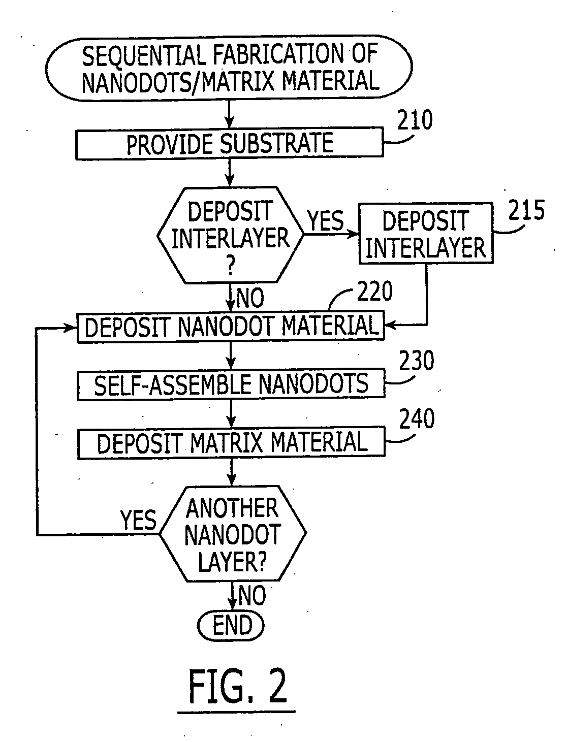
[0076] The sequential formation of self-assembled nickel nanodots and subsequent deposition of matrix materials was performed according to embodiments of the present invention.
[0077] A cross-sectional transmission electron microscope image of a structure formed by the sequential deposition of a nickel nanodot material and the self-assembly of nickel nanodots followed by a deposition of an amorphous aluminum oxide matrix material is shown in FIG. 6. The self-assembled nickel nanodots in the nanodot clusters exhibit an average diameter of 10 nm and the separation between the nanodots is less than 1 nm. The size of the nickel nanodots is uniform, exhibiting a deviation of about 10 percent.
[0078] The structure shown in FIG. 6 was formed by the sequential deposition of nickel nanodots and aluminum oxide matrix material. The deposition was carried out on a silicon substrate at a temperature of about 500° C. in a high vacuum environment (approximately 5×10⁻⁷ Torr) u...
example 2
Simultaneous Deposition
[0082] The simultaneous formation of nickel nanodots in an aluminum oxide matrix on a substrate was performed according to embodiments of the present invention.
[0083] A pulsed laser deposition apparatus 300, such as that illustrated in FIG. 3 was used to simultaneously deposit nickel nanodots in an aluminum oxide matrix material on a silicon substrate 110. The pulsed laser deposition apparatus 300 included a multi-target stainless steel deposition chamber 310, an excimer laser 320, and a turbo molecular pump 330 for maintaining a vacuum in the chamber. A controlled amount of oxygen was also added to the deposition chamber 310 through a controlled gas nozzle. A nickel / aluminum alloy target 340 was placed on a target support 342 parallel to a substrate 110 located on a heater plate 350. The target 340 selected was a commercially available nickel-aluminum alloy including 50 percent by weight nickel and 50 percent by weight aluminum. Nickel was selected as the n...
PUM
| Property | Measurement | Unit |
|---|---|---|
| Diameter | aaaaa | aaaaa |
| Diameter | aaaaa | aaaaa |
| Size | aaaaa | aaaaa |
Abstract
Description
Claims
Application Information