Semiconductor device and method of manufacturing same

a semiconductor and semiconductor technology, applied in the field of semiconductor devices, can solve the problems of loss and deterioration of light emitting elements, and achieve the effect of reducing the generation of heat or efficiently removing or processing the hea

Inactive Publication Date: 2006-11-30
SEMICON ENERGY LAB CO LTD
View PDF99 Cites 54 Cited by
  • Summary
  • Abstract
  • Description
  • Claims
  • Application Information

AI Technical Summary

Benefits of technology

[0013] Hereupon, the invention has its object to efficiently remove or reduc...

Problems solved by technology

Also, all the light generated on the layer containing an organic compound layer is not taken out toward an observer (user) but light is emitted, for example, laterally (direction in parallel to the substrate surface), and as a result, the light emitted laterally i...

Method used


Image

  • Semiconductor device and method of manufacturing same
  • Semiconductor device and method of manufacturing same
  • Semiconductor device and method of manufacturing same

Examples


first embodiment

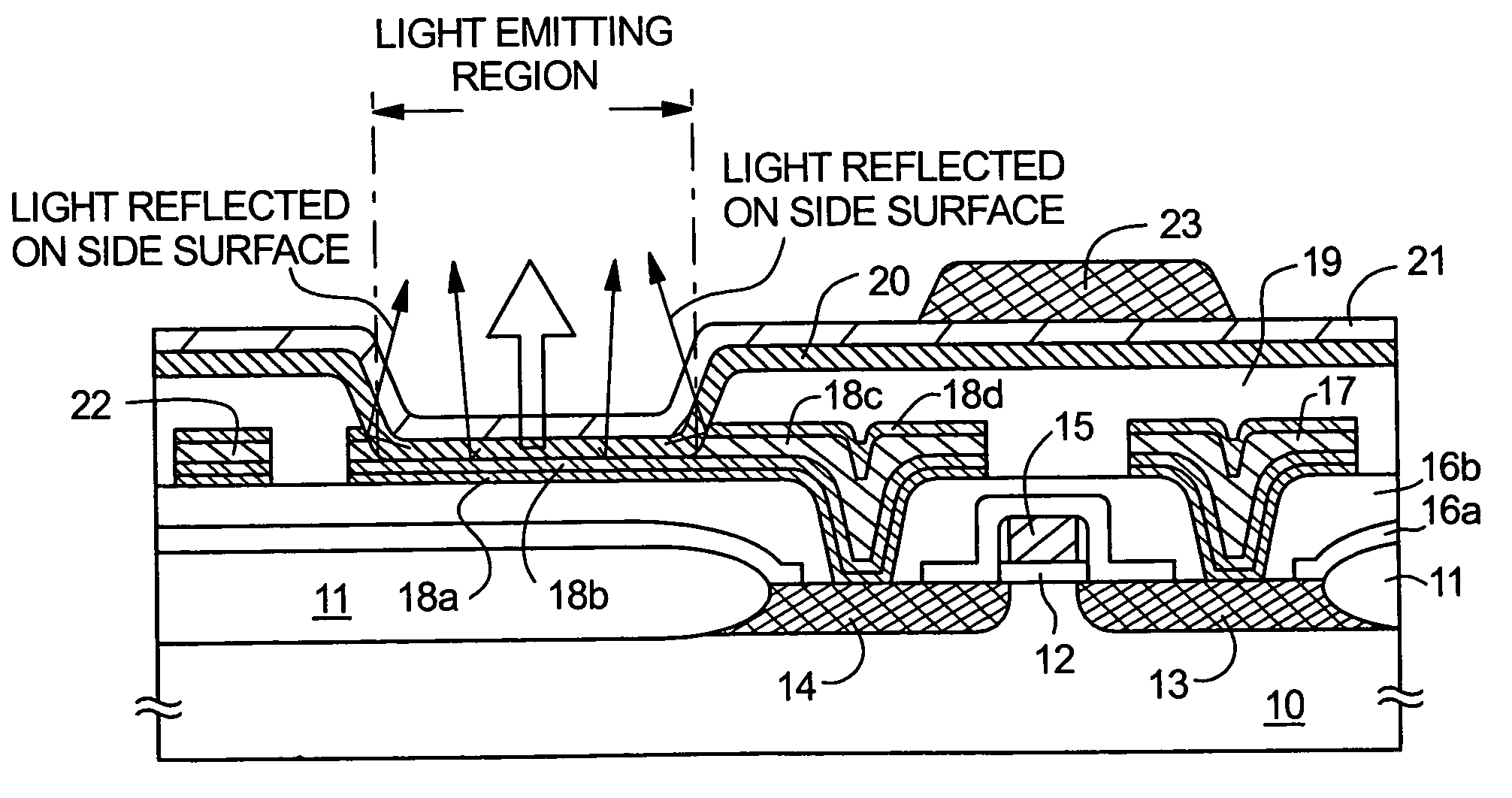
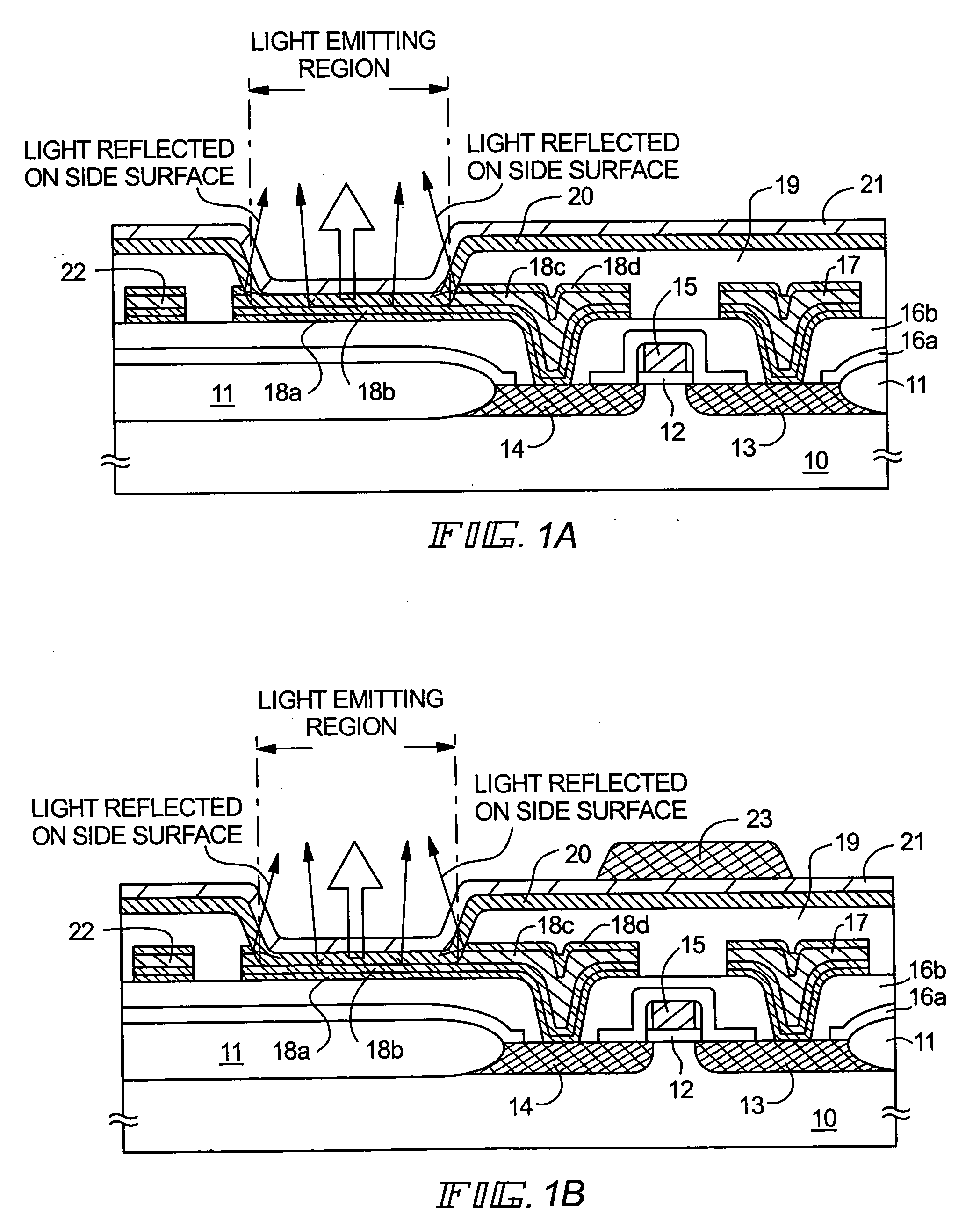
[0065]FIG. 1A is a cross sectional view showing an active matrix type light emitting device (a portion of a pixel). Here, an explanation will be exemplarily given to a light emitting element, in which a layer containing an organic compound composed of a white light emitting polymeric material.

[0066] In FIG. 1A, a FET (PMOSFET) provided on a semiconductor substrate 10 is an element for controlling an electric current flowing to a white light emitting layer 20, the reference numerals 13, 14 denoting source regions or drain regions.

[0067] A N-type or P-type single crystal silicon substrate ((100) substrate, (110) substrate, (111) substrate, or the like), or a high purity semiconductor substrate can be used for a semiconductor substrate 10. Also, for example, a wafer (circular) having a diameter of 200 mm to 300 mm is cut to make a rectangular substrate, and then a FET is formed thereon. Alternatively, multiple patterning may be performed, in which the wafer is divided into sections of...

second embodiment

[0087] An explanation will be given below in FIG. 5A to a method (referred below to as color filter method), in which a white light emitting element and a color filter are combined together.

[0088] The color filter method is a system, in which red, green, and blue light emitting are obtained by forming a light emitting element having an organic chemical compound presenting white light emitting and passing the obtained white light emitting through a color filter.

[0089] There are various methods, by which white light emitting is obtained, and an explanation will be given here to the case where a light emitting layer made of a polymeric material and being formable by coating is used. In this case, doping of a pigment on a polymeric material making the light emitting layer can be carried out by solution adjustment and the layer can be extremely easily obtained as compared with a deposition method, in which codeposition for doping of a plurality of pigments is performed.

[0090] Concrete...

third embodiment

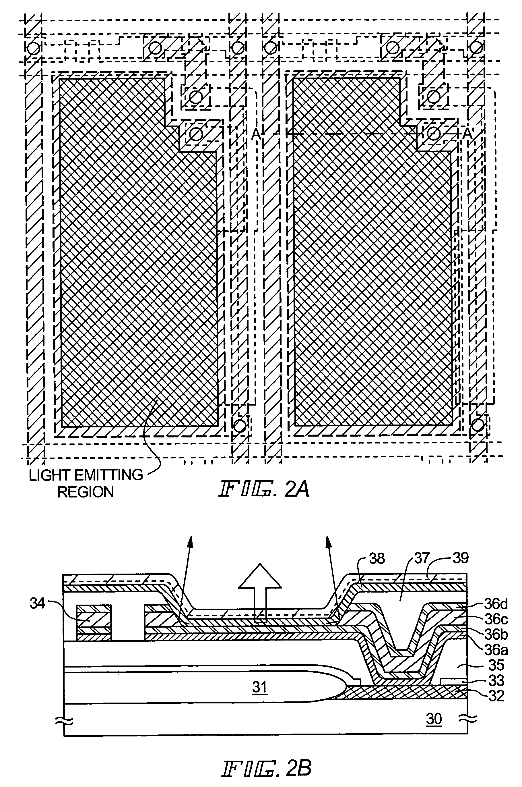
[0104]FIG. 4 shows an example, in which a base insulating film is formed on a semiconductor substrate and a TFT being a kind of FET is formed on the film.

[0105] A N type or P type single crystal silicon substrate ((100) substrate, (110) substrate, (111) substrate, or the like), or a high purity semiconductor substrate can be used for a semiconductor substrate 40. Also, for example, a wafer (circular) having a diameter of 200 mm to 300 mm is cut to make a rectangular substrate, and then a FET is formed thereon. Alternatively, multiple patterning may be performed, in which the wafer is divided into sections of a desired size after a FET and a light emitting element are formed. Also, a chemical compound semiconductor substrate typified by a GaAs substrate, InP substrate, GaN substrate for GaN system epitaxis, SiC substrate, sapphire substrate, ZnSe, or the like may be used for the semiconductor substrate 40. Also, a SOI (Si on Insulator) substrate structure may be formed by means of t...


PUM


Abstract

A FET is formed on a semiconductor substrate, a curved surface having a radius of curvature is formed on an upper end of an insulation, a portion of a first electrode is exposed corresponding to the curved surface to form an inclined surface, and a region defining a luminescent region is subjected to etching to expose the first electrode. Luminescence emitted from an organic chemical compound layer is reflected by the inclined surface of the first electrode to increase a total quantity of luminescence taken out in a certain direction.

Description

BACKGROUND OF THE INVENTION [0001] The present invention relates to a semiconductor device having a circuit composed of field effect transistors (referred below to as FET), and a method of manufacturing the same. In addition, FET referred to in the specification of the present application indicates general elements, in which the basic principle of FET is embodied as an element, and includes MIS FEF, MOS FET making use of oxides for insulator films, and thin film transistors making use of semiconductor thin films. The invention specifically relates to an electronic equipment, on which a semiconductor device having a Light Emitting Diode is loaded as a part. [0002] In addition, a semiconductor device referred to in the specification of the present application indicates devices in general making use of semiconductor characteristics to be able to function, and electro-optic devices, light emitting devices, semiconductor circuits, and electronic equipments are all indicated as semiconduc...

Claims


Application Information

Patent Timeline
IPC IPC(8): H01L31/12H01L27/32H01L51/52
CPCH01L27/3246H01L51/5206H01L51/5221H01L51/5271H01L27/322H01L2251/5315H01L33/0041H01L27/3244H01L27/3211H01L51/529Y02E10/549Y02P70/50H10K59/35H10K59/38H10K59/122H10K50/813H10K50/818H10K50/824H10K50/828H10K50/856H10K50/87H10K2102/3026H10K50/81H10K50/82H10K50/841H10K59/12H10K59/30H10K59/124H10K59/131H10K59/1213H10K71/00H10K77/10H10K59/1201G01J1/4228H01L25/167
Inventor YAMAZAKI, SHUNPEISEO, SATOSHIKUWABARA, HIDEAKI
Owner SEMICON ENERGY LAB CO LTD
Why Eureka
Try Eureka