Image sensor with microcrystalline germanium photodiode layer

a photodiode layer and microcrystalline germanium technology, applied in the field of image sensors, can solve the problems of limiting the achievable pixel count, low collection efficiency, and limited photoresponse of these sensors, and achieve the effect of increasing sensitivity, pixel size and pixel coun

a photodiode layer and microcrystalline germanium technology, applied in the field of image sensors, can solve the problems of limiting the achievable pixel count, low collection efficiency, and limited photoresponse of these sensors, and achieve the effect of increasing sensitivity, pixel size and pixel coun

US20060267054A1Inactive Publication Date: 2006-11-30E PHOCUS

Image

  • Image sensor with microcrystalline germanium photodiode layer
  • Image sensor with microcrystalline germanium photodiode layer
  • Image sensor with microcrystalline germanium photodiode layer

Examples


Embodiment Construction

Two Million Pixel CMOS Sensor

General Description

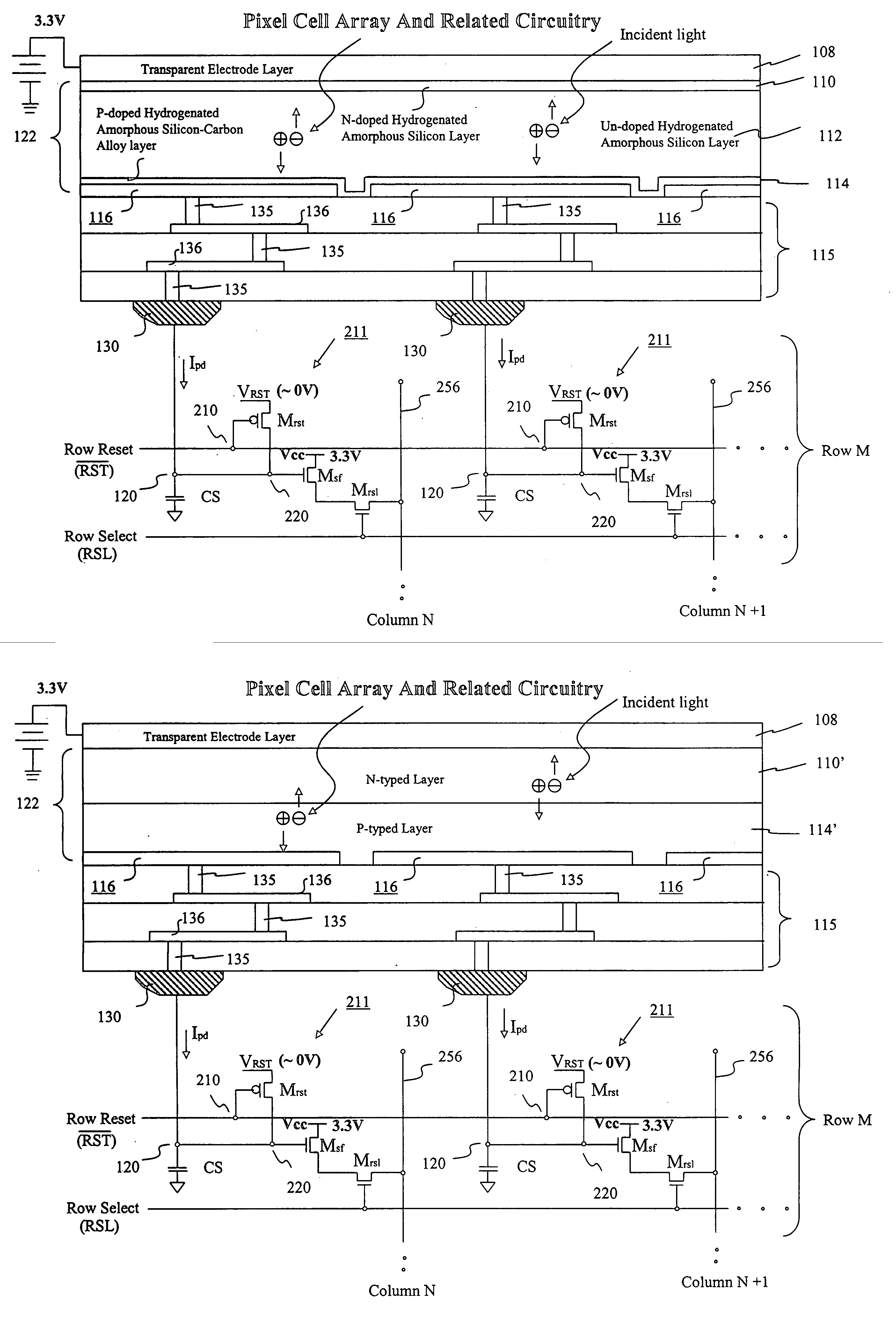
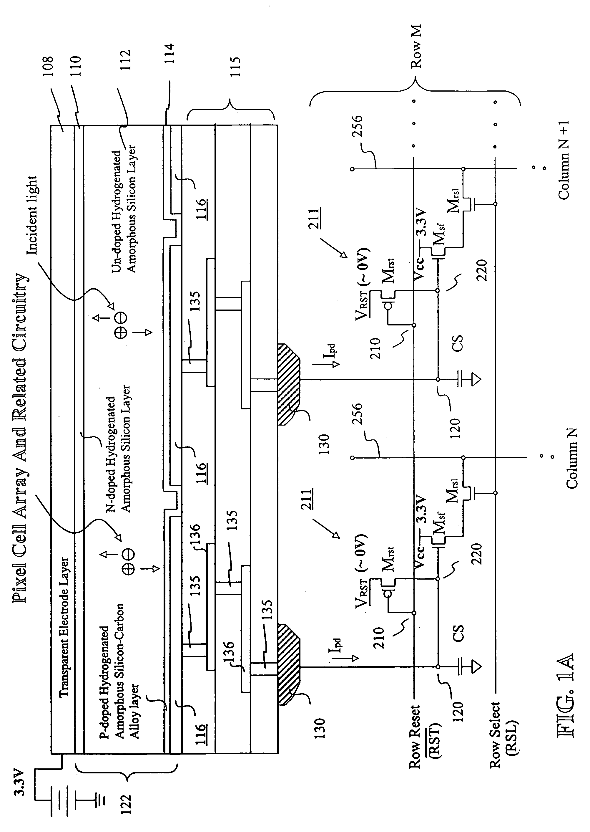
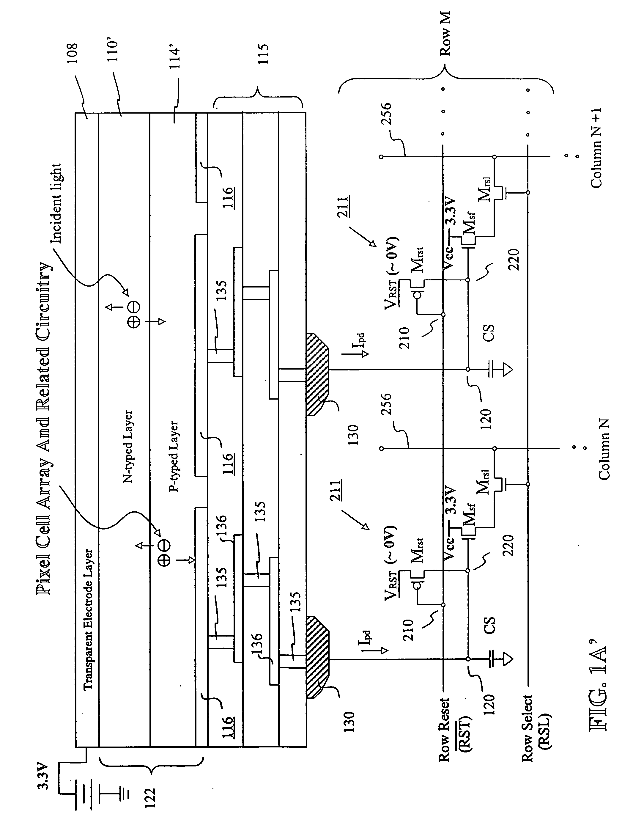
[0037] Some features of a two-million pixel CMOS sensor are shown in FIGS. 1A through 1H. This sensor is fabricated by depositing a multi-layer photodiode structure on top of an electronic readout array that is fabricated using complimentary metal-oxide semiconductor (CMOS) methods commonly utilized in integrated circuit manufacturing. Absorbed photons create charge pairs in the photodiode structure and the liberated electric charge migrates under the influence of an applied electric field to pixel pads in the CMOS readout array where the charges are stored on capacitors, each capacitor representing a pixel. Active pixel circuitry at each pixel produces an amplified voltage proportional to the stored electric charge. CMOS readout circuitry, that may be located at the periphery of each array column, further amplifies and digitizes the pixel signal. Additional pixel circuitry provides digital multiplexing of the digitized pixel signal...


PUM


Abstract

A microcrystalline germanium image sensor array. The array includes a number of pixel circuits fabricated in or on a substrate. Each pixel circuit comprises a charge collecting electrode for collecting electrical charges and a readout means for reading out the charges collected by the charge collecting electrode. A photodiode layer of charge generating material located above the pixel circuits convert electromagnetic radiation into electrical charges. This photodiode layer includes microcrystalline germanium and defines at least an n-layer, and i-layer and a p-layer. The sensor array also includes and a surface electrode in the form of a grid or thin transparent layer located above the layer of charge generating material. The sensor is especially useful for imaging in visible and near infrared spectral regions of the electromagnetic spectrum and provides imaging with starlight illumination.

Description

[0001] This application is a continuation in part of U.S. patent application Ser. No. 10 / 785,833 filed Feb. 23, 2004 which was a continuation of patent application Ser. Nos. 10 / 746,529, filed Dec. 23, 2003; Ser. No. 10 / 648,129 filed Aug. 26, 2003; Ser. No. 10 / 371,618, filed Feb. 22, 2003; Ser. No. 10 / 229,953 filed Aug. 27, 2002; Ser. No. 10 / 229,954 filed Aug. 27, 2002; Ser. No. 10 / 229,955 filed Aug. 27, 2002; Ser. No. 10 / 229,956 filed Aug. 27, 2002 and Ser. No. 10 / 072,637 filed Feb. 5, 2002. This application also claims the benefit of Provisional Patent Application Ser. No. 60 / 656,236 filed Feb. 24, 2005. This patent application relates to image sensors and in particular to broad spectrum image sensors covering spectral ranges within the visible and near infrared spectral ranges.BACKGROUND OF THE INVENTION [0002] The prior art includes a variety of image sensors. Image sensors operating in the visible and near infrared spectrums have widespread utility for military and commercial ap...

Claims


Application Information

Patent Timeline
30 Nov 2006
Publication
US20060267054A1
IPC
H01L31/113
CPC
H01L27/14632; H01L27/14643; H01L27/14687; H01L31/0322; Y02E10/546; H01L31/105; H01L31/1055; H01L31/1808
Inventors
MARTIN, PETER; ENGELMAN, MICHAEL G.