Trech-type vertical semiconductor device having gate electrode buried in rounded hump opening

a technology of gate electrodes and vertical semiconductors, which is applied in the direction of semiconductor devices, basic electric elements, electrical equipment, etc., can solve the problem of inability to avoid avalanche breakdown phenomena, and achieve the effect of reducing breakdown voltage and increasing on-resistan

Inactive Publication Date: 2006-11-30
RENESAS ELECTRONICS CORP
View PDF7 Cites 49 Cited by
  • Summary
  • Abstract
  • Description
  • Claims
  • Application Information

AI Technical Summary

Benefits of technology

[0010] In the above-described third prior art semiconductor device, however, it is impossible to avoid an avalanche breakdown phenomenon. That is, since the base region does not reach the rounded hump openings of the trenches, the breakdown current flows to turn ON the parasitic bipolar transistor. Also, since the depth of the trenches is larger than that of the base region, a non-flat depletion region is generated at the bottom of the base region caused by a reverse bias voltage applied thereto, which would decrease the breakdown voltage. Further, since the current path of the MOS transistor is relatively long, its ON-resistance is increased.

Problems solved by technology

In the above-described third prior art semiconductor device, however, it is impossible to avoid an avalanche breakdown phenomenon.

Method used


Image

  • Trech-type vertical semiconductor device having gate electrode buried in rounded hump opening
  • Trech-type vertical semiconductor device having gate electrode buried in rounded hump opening
  • Trech-type vertical semiconductor device having gate electrode buried in rounded hump opening

Examples


first embodiment

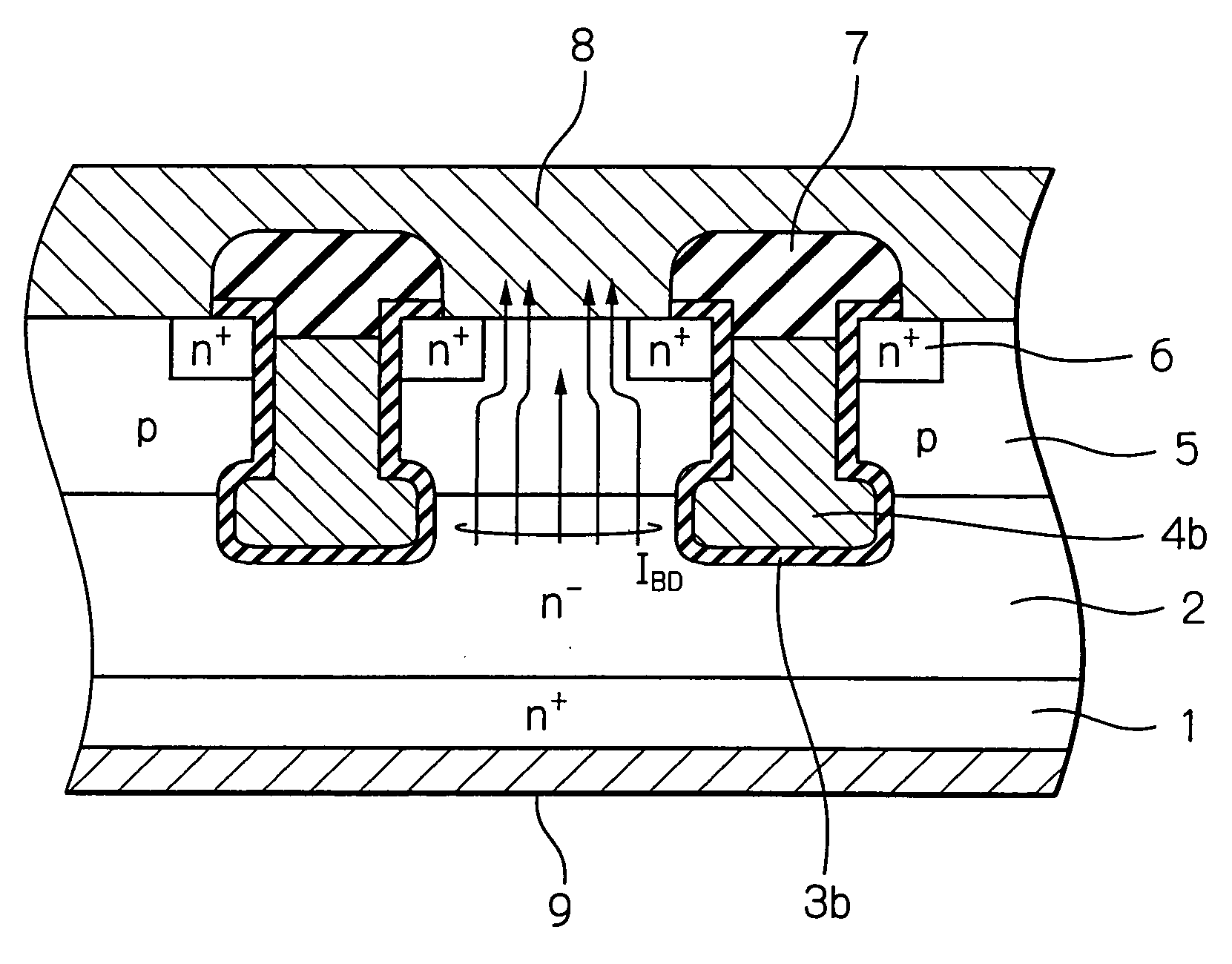
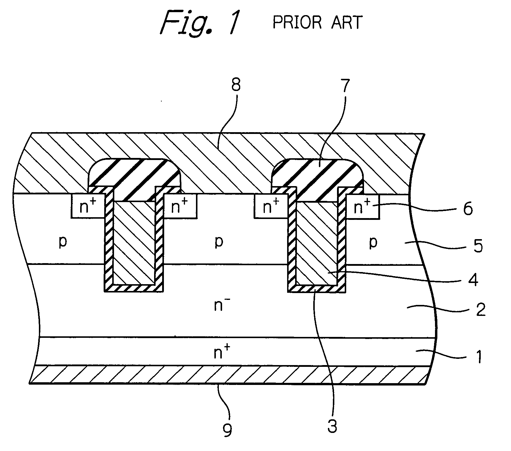
[0034] In FIG. 7, which illustrates the semiconductor device such as a trench-type vertical MOS transistor according to the present invention, rounded hump openings are provided on the bottoms of trenches within a region between the n−-type epitaxial silicon layer 2 and the p-type base region 5 of FIG. 1, so that the gate silicon dioxide layers 3 and the gate electrodes 4 of FIG. 1 are replaced by gate silicon dioxide layers 3b and gate electrodes 4b which have rounded humps within the region between the n−-type epitaxial silicon layer 2 and the p-type base region 5. In more detail, one trench is constructed by an opening OP1 with a width W1 and a rounded hump opening OP2 with a width W2 larger than the width W1 below the opening OP1. The rounded hump opening OP2 has a curvature radius of larger than 0.1 μm. The bottom of the p-type base region 5 reaches the rounded hump opening OP2 of the trench. Thus, the current concentration is relaxed as illustrated in FIG. 8, which would suppr...

second embodiment

[0051] In FIG. 10, which illustrates the semiconductor device such as a trench-type vertical IGBT according to the present invention, the n+-type monocrystalline silicon substrate 1, the n−-type epitaxial silicon layer 2, the gate silicon dioxide layer 3b, the gate electrodes 4b, the p-type base region 5, the n+-type source impurity diffusion regions 6, the insulating layers 7, the source electrode 8 and the drain electrode 9 of FIG. 7 correspond to an n+-type buffer 31, an n−-type base layer 32, agate silicon dioxide layer 33b, gate electrodes 34b, a p-type base region 35, an n+-type emitter impurity diffusion regions 36, insulating layers 37, an emitter electrode 38 and a collector electrode 39, respectively. Also, an n+-type collector region 30 is provided between the n+-type buffer 31 and the collector electrode 39.

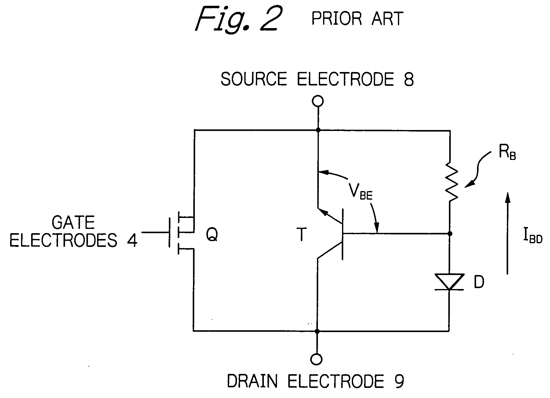
[0052] As illustrated in FIG. 11, which is an equivalent circuit diagram of the semiconductor device of FIG. 10, the n+-type emitter impurity diffusion regions 36, th...


PUM


Abstract

In a semiconductor device including a gate electrode buried in a trench of the device, the trench is constructed by a first opening with a uniform width the same as that of an upper portion of the first opening and a second opening beneath the first opening with a width larger than the uniform width. A bottom of a base region adjacent to the trench is adjacent to the second opening.

Description

BACKGROUND OF THE INVENTION [0001] 1. Field of the Invention [0002] The present invention relates to a trench-type vertical semiconductor device such as a trench-type vertical metal oxide semiconductor (MOS) transistor and a trench-type vertical insulated gate bipolar transistor (IGBT). [0003] Generally, since trench-type vertical MOS transistors and IGBTs are easy to control and have negative temperature coefficient ON-currents, they have been used as power semiconductor devices for driving inductance loads such as motors and solenoid values in automobiles. When such inductance loads are driven by the above-mentioned MOS transistors or IGBTs, it is important that an avalanche breakdown phenomenon caused by the inductance loads should be suppressed. [0004] 2. Description of the Related Art [0005] A first prior art trench-type vertical semiconductor device is constructed by gate electrodes buried in trenches each of which has a uniform width. In this case, the bottom of a base region...

Claims


Application Information

Patent Timeline
Patent Type & Authority Applications(United States)
IPC IPC(8): H01L29/94H01L21/336
CPCH01L29/4236H01L29/7813H01L29/7397H01L29/66734
Inventor MATSUURA, NAOKI
Owner RENESAS ELECTRONICS CORP
Why Eureka
Try Eureka